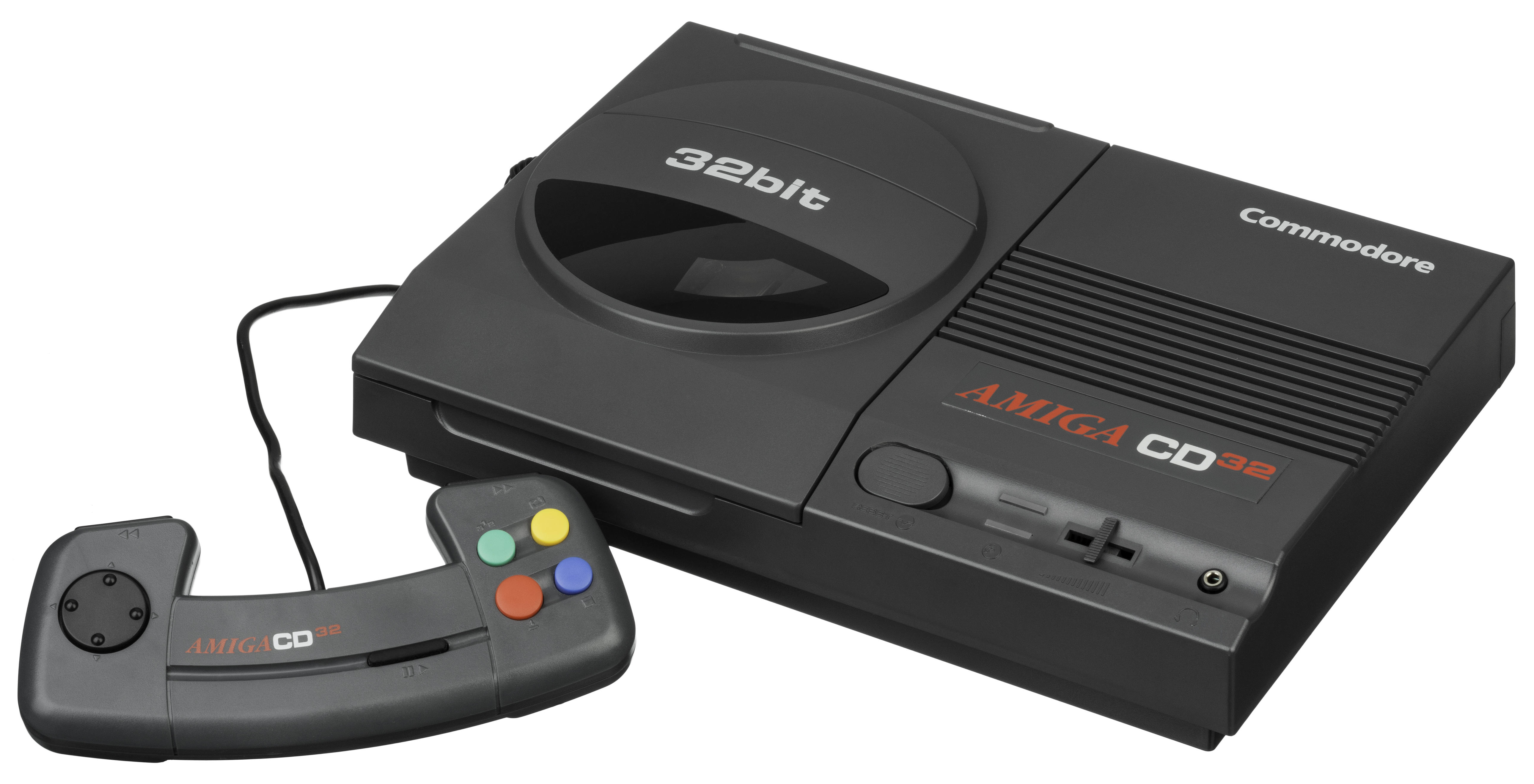
Throughout July, for Reasons of Science, I found myself playing the Amiga's last great mascot platformer,
Brian the Lion, on the Amiga CD32. If you're not familiar with the CD32, it's a 32-bit CD-ROM based console (the first of the misadventurous 16/32-bit
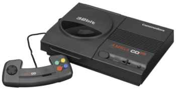
fourth-and-a-half generation consoles released in the UK). And it looks a bit like this.
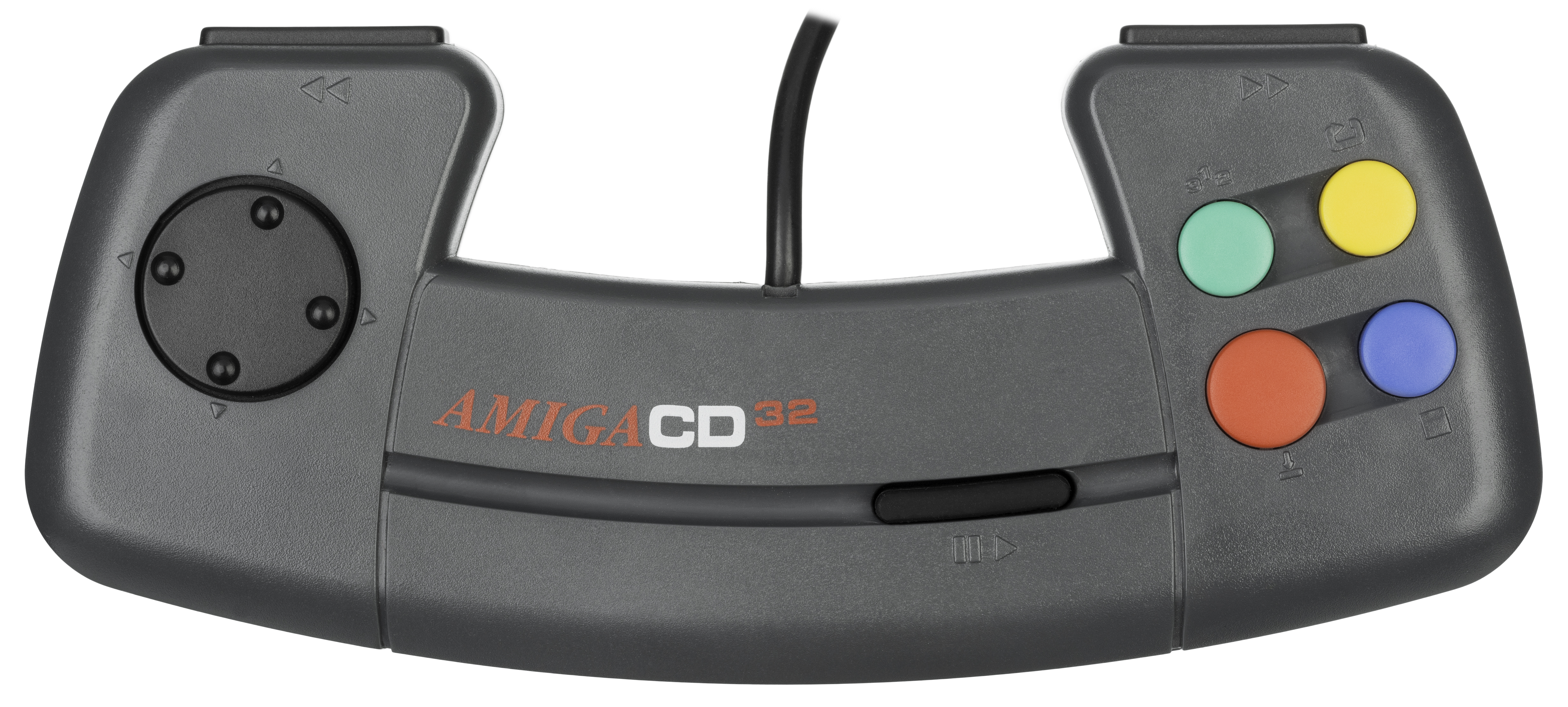
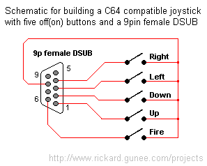
It's an Amiga 1200, magically transmuted into the form of a video game console. It has two 9-pin controller ports on the side, which are the same as those found on the Amiga home computer series (but not the CDTV, even though it's an A500, though Commodore pretended it wasn't). As such, it's compatible with all Amiga controllers, such as the magnificent, clicky, and magnificently clicky Zipstik joystick, and two button pads like the Sega Master System. However, since it's a nifty video games machine, it has its own special, completely-incompatible-with-everything-else, controller. That odd, telephone/dogbone looking thing, there.
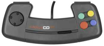
The CD32 pad has seven buttons: four coloured face buttons, two shoulder buttons and a central button. The face buttons are coloured Red, Blue, Yellow and Green and, like the rest of the buttons on the controller, are decorated with video-player-like emblems as if you could play videos on the system. Which you can't, really. The shoulder buttons are not labelled L and R, instead game manuals refer to them as the 'top left feature button' and other adorably weird names CHECK. (Except for
Guardian, which is sensible.)
I'm going to call the shoulder buttons FF (on the right) and Rew (on the left), because they remind me of the Time Controls from
Blinx the Time Sweeper.
The directional pad is digital and has four directions: Up, Down, Left and Right. It's circular, somewhat like a Mega Drive pad, except five billion times more fragile.
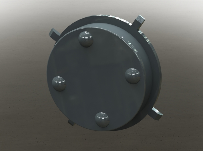
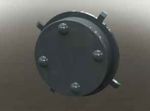
Replacement directional pad design by Ndo Design.
https://www.shapeways.com/product/XLKEBL3WQ/commodore-amiga-cd32-controller-d-pad
It's a disc shape with protruding fingers on its base to lock it into a notched circular holder inside the pad. With minimal use (and thirty years of age) the notches can break, freeing the disc to rotate underneath your thumb, which moves the cardinal direction studs and contacts underneath out of position, making the pad nearly unusable.
That's no good, especially if you just want to be a lion.
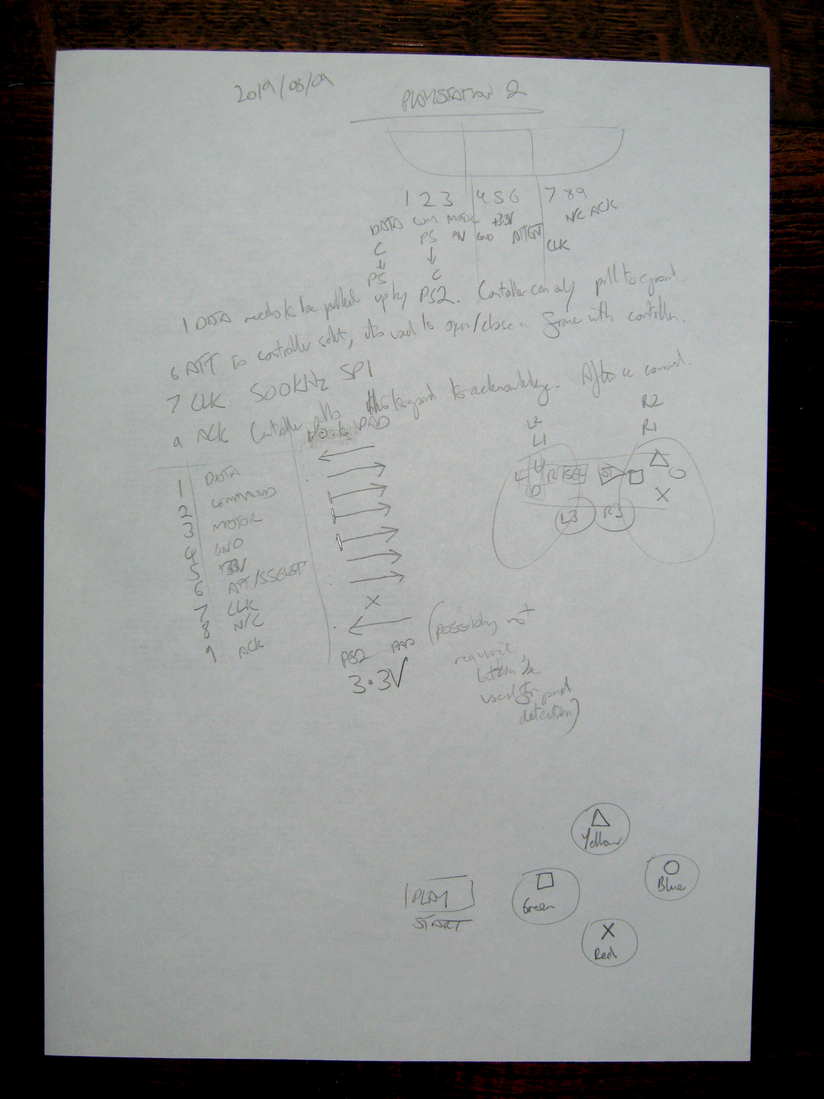
I looked up possible ways to fix the pad, along with schematics for it. I wondered how difficult it would be to build a new pad from scratch completely - which didn't seem to be particularly difficult as it consists of eleven contacts and two standard logic chips. Designing and 3D printing a new pad case or D pad was possible, even plausible, but a little beyond what I felt like doing at this point.
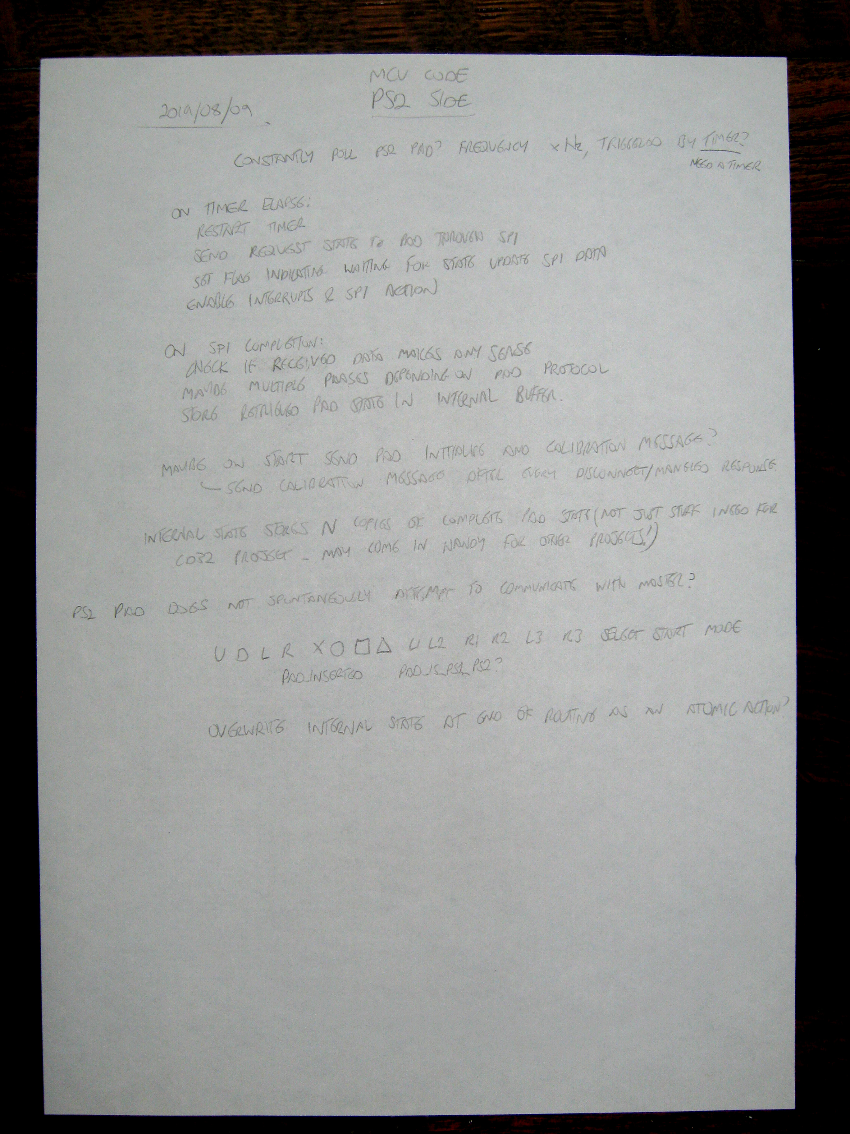
I hadn't done any microcontroller work in a while and also wondered if I could simulate the function of those chips in software. Since Playstation pads and their
cheap-but-effective clones are still being manufactured by the million to this day (2019), a Playstation to CD32 convertor was the natural choice.
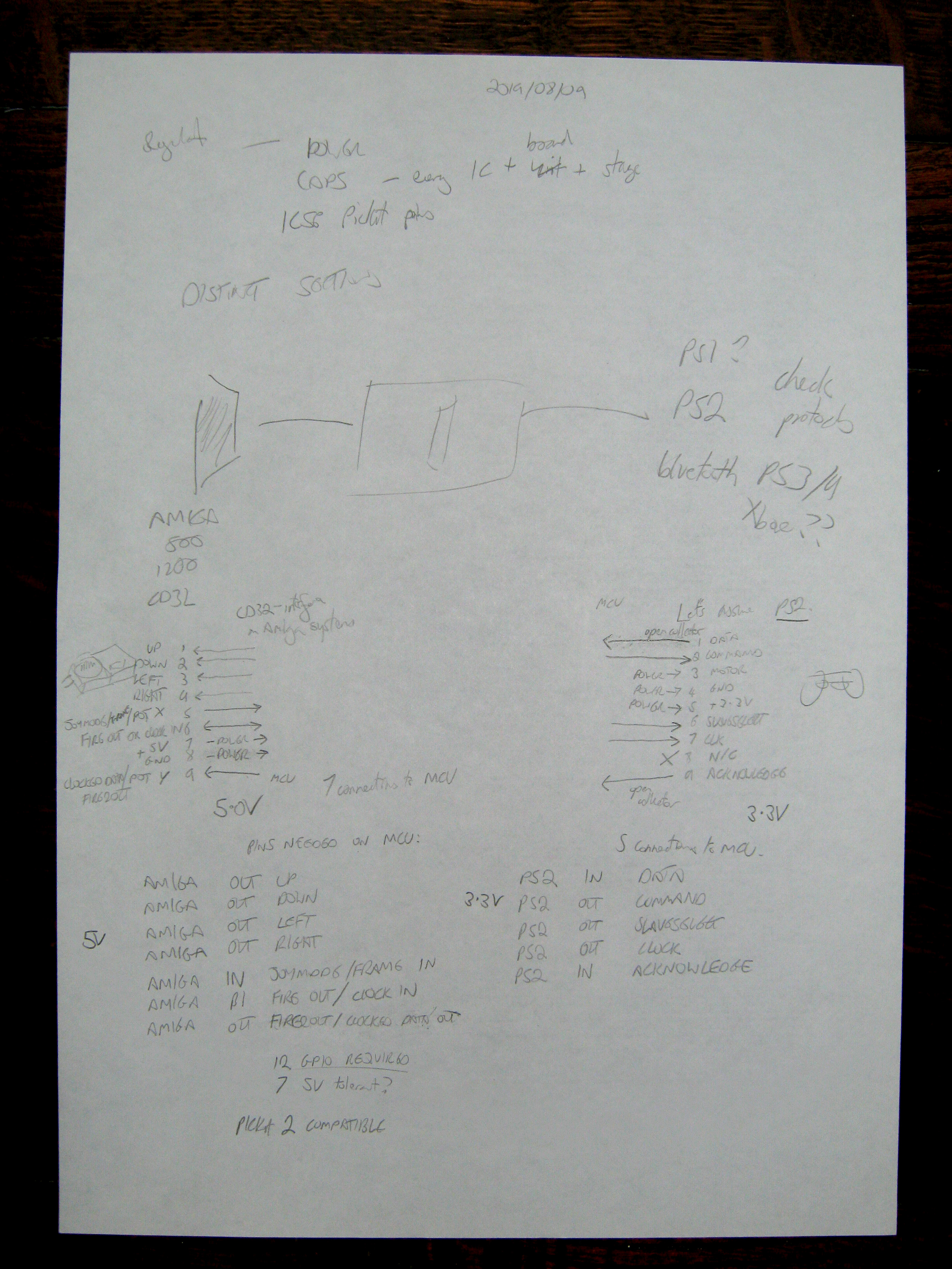
The first thing to do is to research absolutely everything.
• How does a CD32 power a CD32 controller (if it needs to)?
• How does a CD32 console talk to a CD32 controller?
• How does a Playstation power a Playstation pad?
• Can a CD32 power a Playstation pad?
• How does a Playstation console talk to a Playstation pad?
• Can a CD32 power a Playstation pad together with some guys that translates the messages?
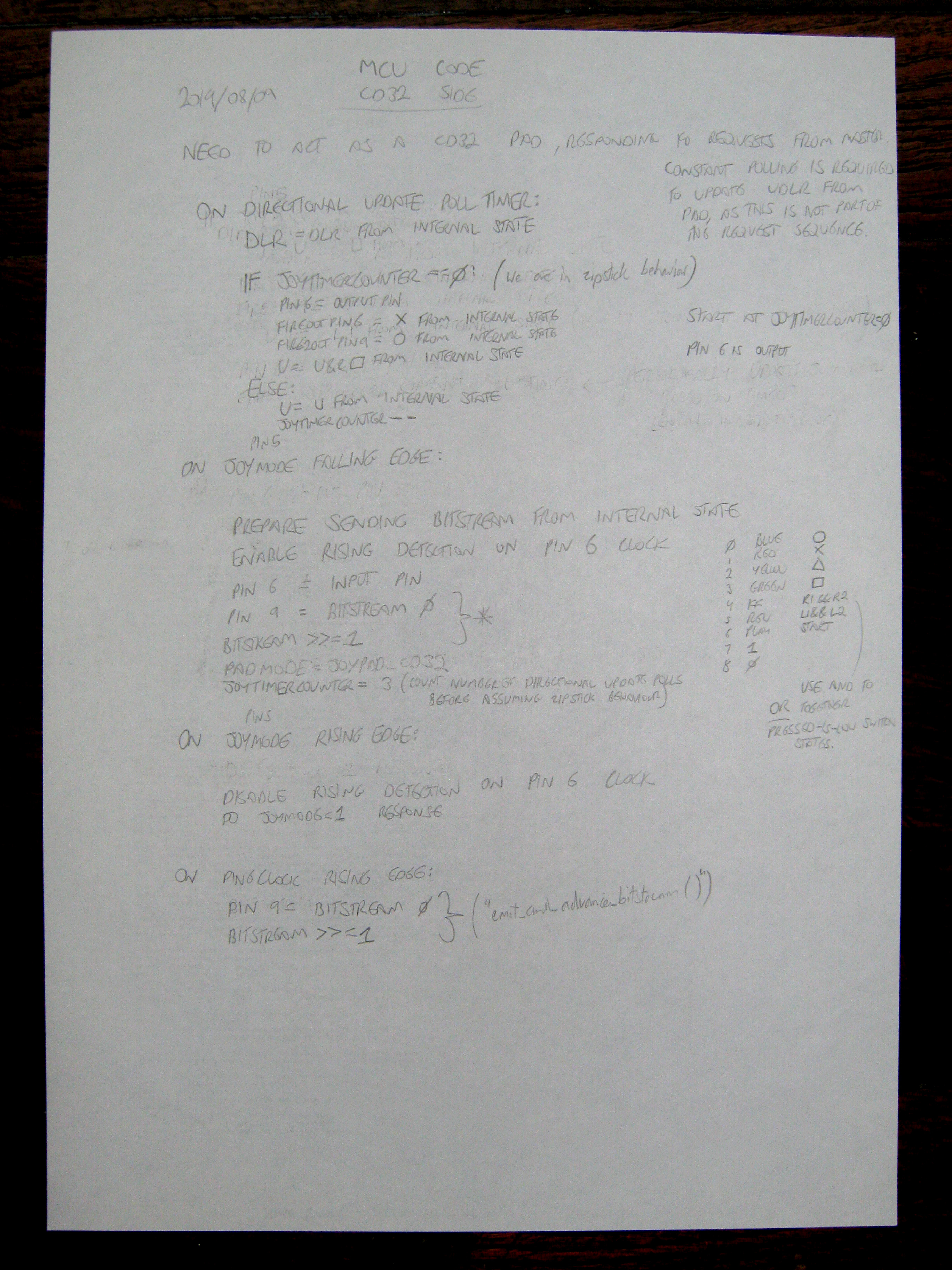
The CD32 stuff
The first two questions were answered by searching for schematics and pinouts of a CD32 pad online. I could have (and should have) taken my own one apart to see if I could fix the broken directional pad at the same time, but having bits of irreplaceable plastic raining down on my lap would've just depressed me.
Here's a mirror of Gerd Kautzmann's CD32 controller page. (
http://gerdkautzmann.de/cd32gamepad/cd32gamepad.html)
Oddly enough it seems to exist because Gerd was frustrated that the directional pad was on the left side of the pad, which didn't suit their grip, rather than the thing being an unresponsive, fragile, irreplaceable pile of tat.
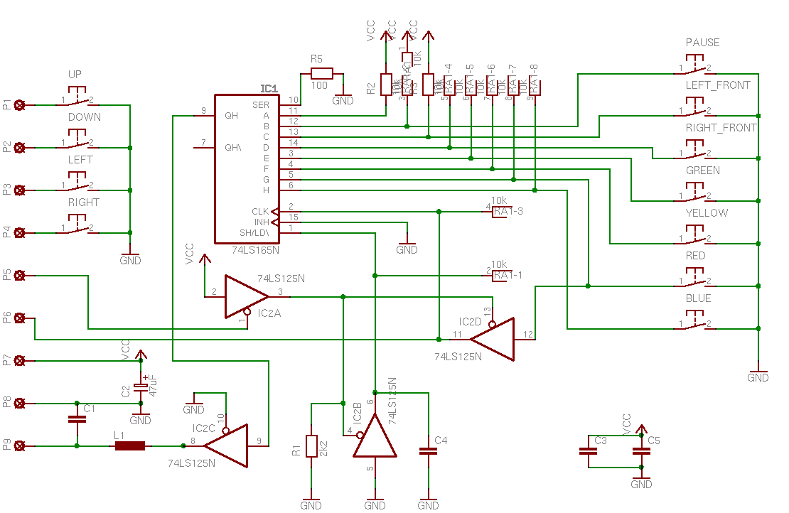
They have a wonderful, if needlessly confusing, schematic of the pad:
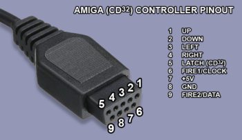
This pinout from
the KTRL CD32 project is a definitive CD32 pinout:
The mechanics of the CD32 can be mystifying at first, but I've got to master them if I want to create a device that speaks the same protocol.
For example, in isolation, this is meaningless:

By using these sources of information together with a bit of background information about the Amiga, we can determine what the CD32 pad does and why.
First, here's a basic description of a simple one-button Amiga joystick:
• The function of the joystick is to allow the user to input Up, Down, Left, Right, Fire or any combination of these. These are on/off inputs.
• All five inputs are implemented as switches within the joystick linking pins 1, 2, 3, 4 and 6 from the Amiga to the ground connection.
• The Amiga contains internal pull-ups which pull the voltages at these pins high by default.
• When the buttons are pressed or directions are pulled on the joystick, switches to ground are closed, pulling the voltages at these pins low.
• This means that when the switches are open, the voltage is high. When the switches are closed, the voltage is low. These states are read as 1 and 0 by the Amiga hardware.
On a two-button joystick or two-button mouse, pin 9 provides Fire 2/Right Mouse. On a three-button joystick or a three-button mouse, pin 5 provides Fire 3/Middle Mouse.
As a schematic, the joystick itself looks like this:

If you wanted to play
B.C. Kid with two buttons, this would be all you need!
However, this doesn't explain how the CD32 is able to provide eleven unique binary inputs to the Amiga (Up, Down, Left, Right, Blue, Red, Yellow, Green, FF, Rew and Pause) with only seven data lines.
The secret is that the above explanation is a simplification!
It's true that the Up, Down, Left and Right inputs to the Amiga are simple pulled-up pins that are switched to ground, but the three Fires aren't.
Let's have a look at
the Amiga schematics at https://www.amigawiki.org/doku.php?id=en:service:schematics.
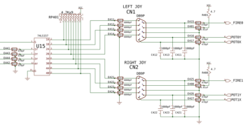
This somewhat-combed spaghetti shows a few things:
• The two joystick ports are identical.
• The box labelled RP401 is a resistor array that pulls all the directional input pins up.
• The directional inputs are read using a uni-directional 74157 multiplexer so the Amiga can't set any pin high or low to change the behaviour from the described.
• The three Fire inputs link internally to points labelled
_FIRE0,
POT0Y and
POT0X within the Amiga chipset.
_FIRE* links to a CIA on an A500 (Akiko on a CD32), and
POT** link to Paula in both an A500 and a CD32. (The
POT** pins are used for two axes of analogue input on each joystick port, for paddles and pens and other inventions.) Functionally, this means that all three can act as general purpose bidirectional IO pins, and can be configured as output low (sinking current), output high (sourcing current) or High-Z (no effect on output voltage, reading value from external effects), and can be read during any of these settings.
This means that with some fiddling magic, the Amiga can actively perform a protocol to read values from the controller.
Here's the pad schematic again:
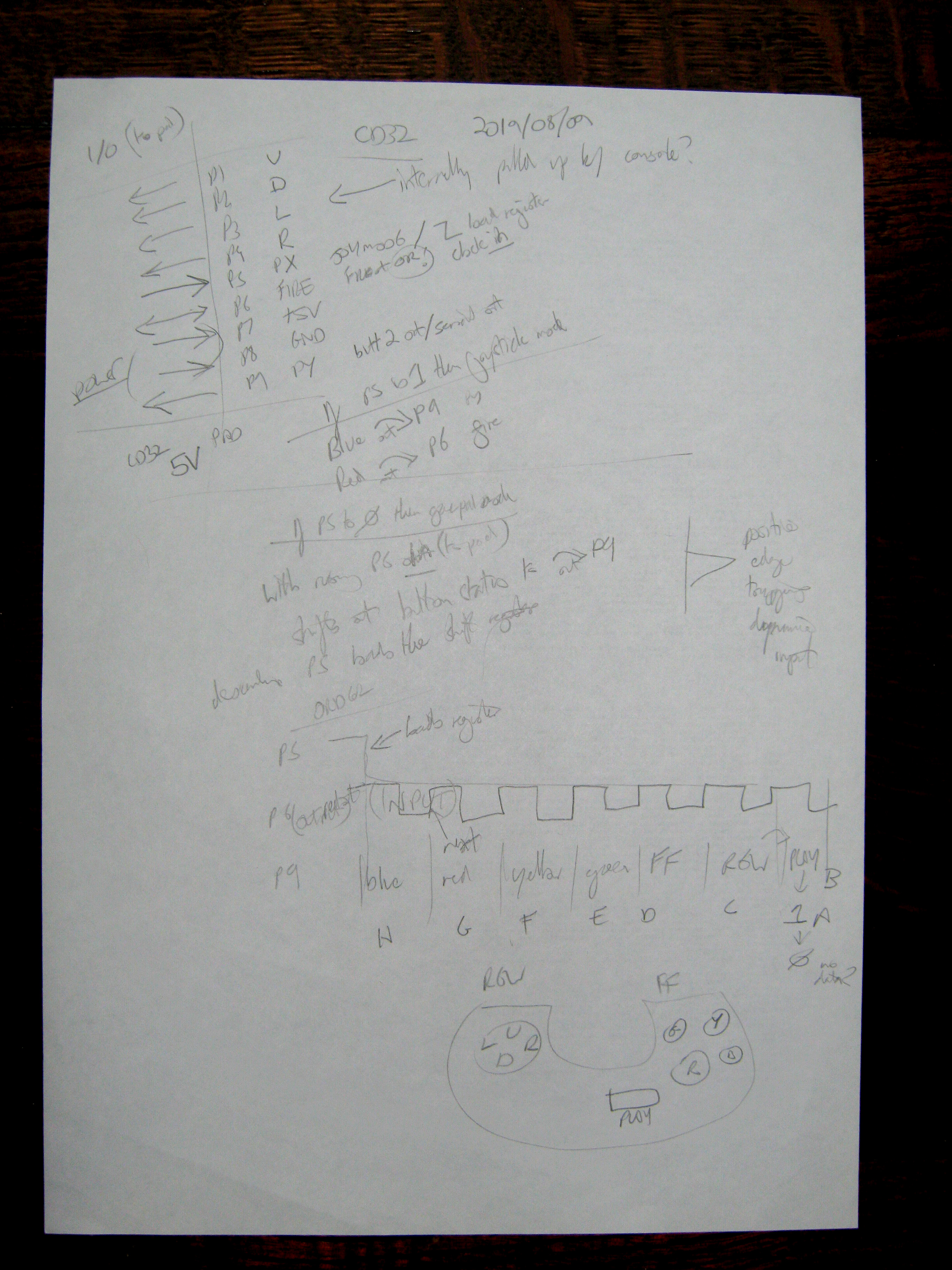
First, I'll define a table of pin names and roles:
| Pin Number | Amiga Name | CD32 Pad Role | Directionality |
| 1 | UP | UP | Controller --> System |
| 2 | DOWN | DOWN | Controller --> System |
| 3 | LEFT | LEFT | Controller --> System |
| 4 | RIGHT | RIGHT | Controller --> System |
| 5 | POT0X | JOYMODE/FRAME | Controller <-- System |
| 6 | FIRE0 | FIRE1OUT/CLOCKIN | Controller <-> System |
| 7 | +5V | +5V | Controller <-- System |
| 8 | GND | GND | Controller <-- System |
| 9 | POT0Y | FIRE2OUT/DATAOUT | Controller --> System |
• The Up, Down, Left and Right inputs on the directional pad are just switches to ground, as in a normal joystick.
• There is a connection from pin 7
+5V, so the pad requires/uses the power supplied by the joystick port.
• The upper left IC is a 74LS165N, which is
a 74165 low power schottky 8-bit parallel to serial shift register in a DIP package.
• The triangular symbols are the gates of a 74LS125N,
a 74125 low power schottky active-low tri-state non-inverting buffer in a DIP package.
Let's assume that pin 5
JOYMODE/FRAME is set to High by the Amiga:
• If pin 5
POT0X JOYMODE/FRAME is set to High, this sets gate
IC2A to tri-state, which allows the enables of
IC2D and
IC2B to be pulled to ground and enabled.
• When
IC2D is enabled, the Red input is buffered through
IC2D and out towards pin 6 as
FIRE1OUT.
• When
IC2B is enabled, it passes Low to the
SH/_LD input of the shift register, putting it into Load mode, making it update internally with the states of the Blue, Red, Yellow, Green, FF, Rew and Pause buttons.
• With the shift register in Load mode, the current state of the Blue button linked to input H is passed directly to the shift register output.
• The output of the shift register is buffered by an always-on buffer
IC2C towards pin 9 as
FIRE2OUT.
Ultimately, this means that:
• If the
JOYMODE pin is set high by the Amiga, the pad is set to a
dumb joystick mode. The states of Fire 1 (Red) and Fire 2 (Blue) are reported to the Amiga by grounding the
FIRE1OUT and
FIRE2OUT pins respectively as if Fire 1 and Fire 2 were simple switches to ground.
This is exactly the behaviour of a two-button joystick or a Sega Master System pad. Great!
Now let's assume that pin 5
JOYMODE/FRAME was High, but is now set to Low by the Amiga:
• If pin 5
POT0X JOYMODE/FRAME is set to Low, this sets gate
IC2A to enabled, which passes a High signal to the enables of
IC2D and
IC2B, disabling them.
• When
IC2D is disabled, the
RA1-3 resistor is free to pull the
CLK input of the shift register High, unless it is pulled low by pin 6 as
FIRE1OUT/CLOCKIN.
• When
IC2B is disabled, the
RA1-1 resistor is free to pull the
SH/_LD input of the shift register high, putting it into Shift mode, freezing the internal states of the eight inputs with the states of the Blue, Red, Yellow, Green, FF, Rew and Pause buttons, followed by a 1 (High) due to
R2.
• The output of the shift register is buffered by an always-on buffer
IC2C towards pin 9 as
DATAOUT.
Now the pad's behaviour is different. Pin 6
FIRE1OUT/CLOCKIN is being used as an input to the controller, and pin 9
FIRE2OUT/DATAOUT is sending the output of the shift register.
Now this table makes more sense. :)
• The Amiga can now read the value of the Blue button at pin 9
DATAOUT.
• On the rising edge of pin 6
CLOCKIN (controlled by the Amiga), the value at pin 9
DATAOUT will change to the next input, which is Red.
• On each new rising edge of pin 6
CLOCKIN, the next input will be presented, in this order: Blue, Red, Yellow, Green, FF, Rew, Pause, 1, 0, 0, 0...
The sequence of inputs returned can be seen on the schematic as pins
H through
A on the shift register, with the
SER shift-in input being used to provide an endless sequence of zeroes (Lows) once the eight variables have been exhausted.
This means that:
• If the
JOYMODE pin is set low, the pad is set to
seven button shift register mode. On the falling edge of the
JOYMODE signal, the states of the Blue, Red, Yellow, Green, FF, Rew and Pause buttons are captured, and the state of the Blue button is presented on
FIRE2OUT/DATAOUT.
FIRE1OUT/CLOCKIN is treated as an input signal. On each rising edge of
FIRE1OUT/CLOCKIN, a new button state is shifted onto the
FIRE2OUT/DATAOUT line in a set sequence. When all seven buttons have been shifted, a final 1 signal is reported, followed by endless 0s.
In both modes
JOYMODEs, the Up, Down, Left and Right inputs are exactly the same as those of a dumb joystick.
To summarise:
• The CD32 pad has two modes, determined by the state of the pin 6
JOYMODE pin. This pin is controlled by the Amiga, and is one of the three bidirectional pins the Amiga joyport has.
• If the
JOYMODE pin is set High by the Amiga, the pad is set to a
dumb joystick mode. The states of Fire 1 (Red) and Fire 2 (Blue) are reported to the Amiga by grounding the
FIRE1OUT and
FIRE2OUT pins respectively as if Fire 1 and Fire 2 were simple switches to ground.
• If the
JOYMODE pin is set Low, the pad is set to
seven button mode.
CLOCKIN is treated as an input signal. On each rising edge of
CLOCKIN, a new button state is shifted onto the
DATAOUT line in a set sequence. When all seven buttons have been shifted, a final 1 signal is reported, followed by endless 0s.
Notice that the
FIRE1OUT/CLOCKIN pin is bidirectional in this protocol, and its role changes based on
JOYMODE. Specifically, it is an output if
JOYMODE is high, and an input if
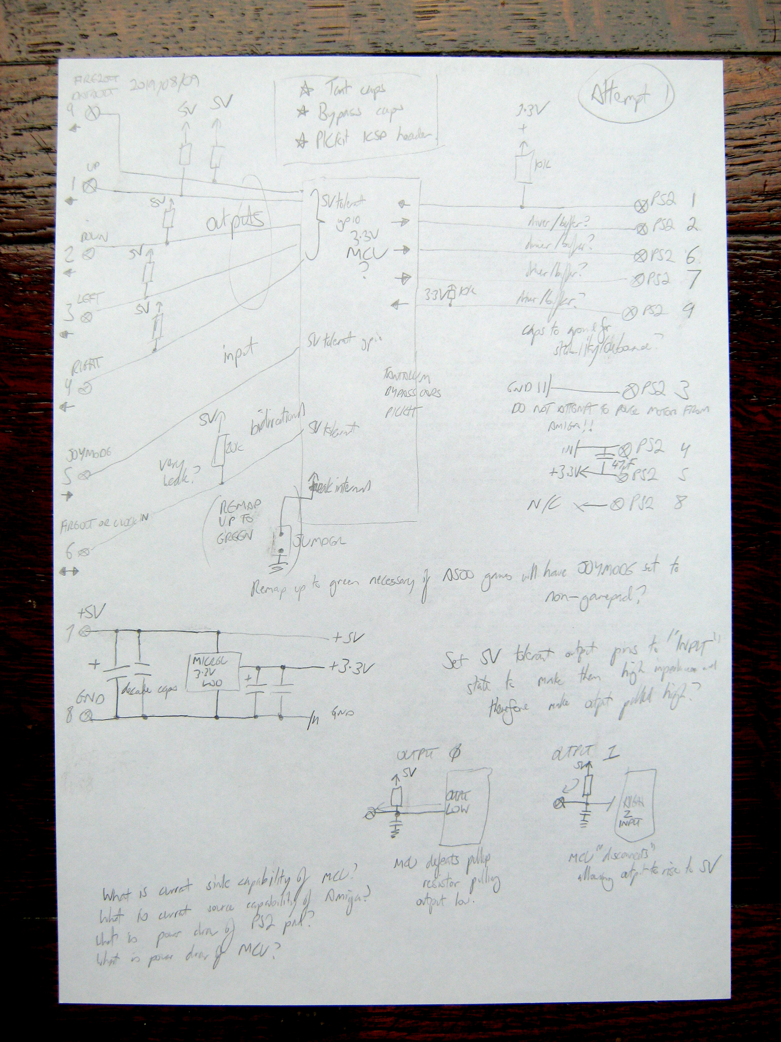
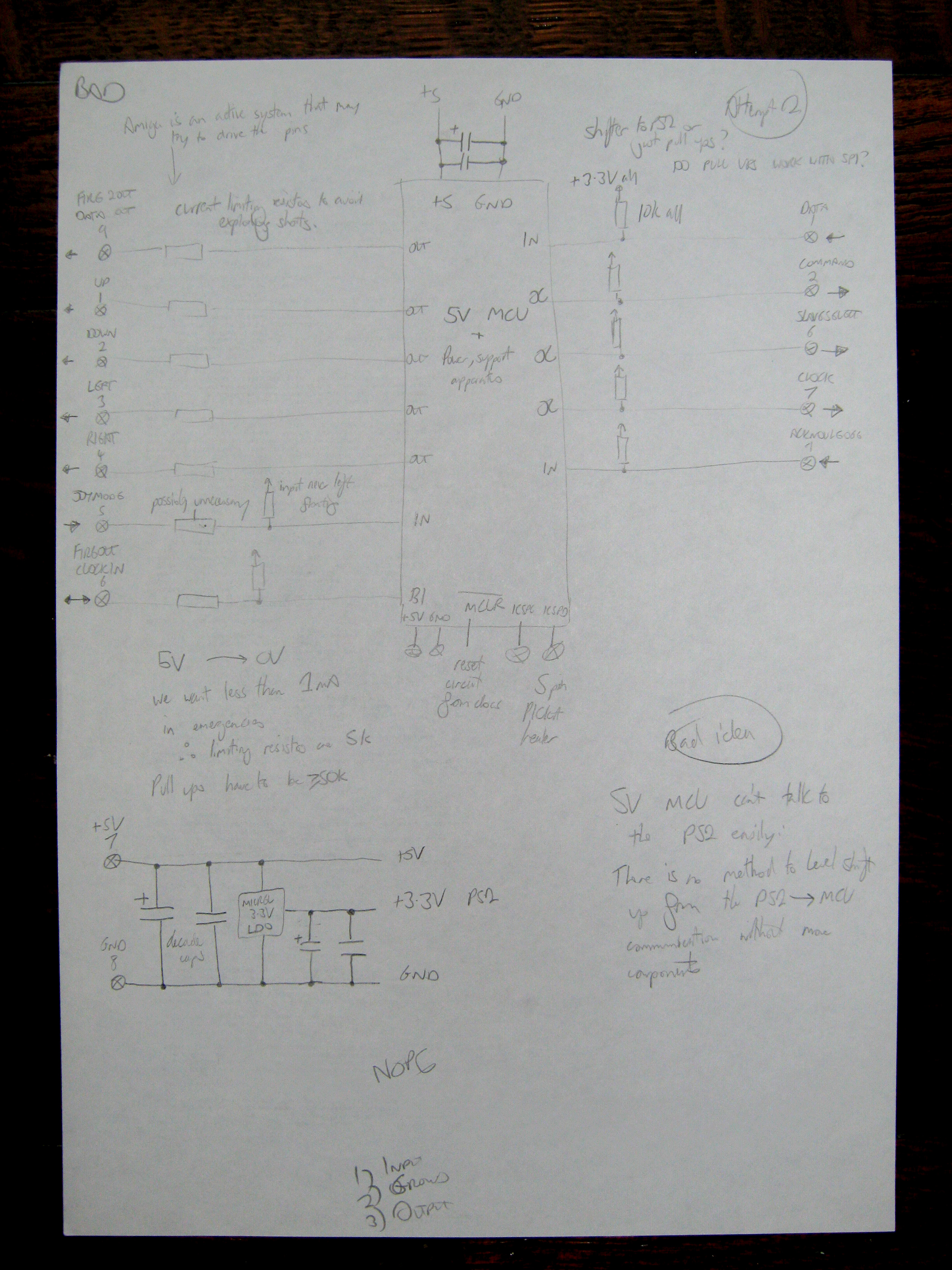
JOYMODE is low. Because the Amiga can change the state of pins 5, 6 and 9 on each joyport at any time, and because the system runs arbitrary game/program code directly with no hypervisor or hardware locks, the states of these pins are able to change at any time. This means it very possible and likely for a device plugged into the joyport to cause bus contention, with both the device and the Amiga attempting to drive one of these pins at the same time if it doesn't react properly. This is Not Good.
I asked on the
English Amiga Board for information about the electrical characteristics of the Amiga's joystick ports. They supply 5 volts through a 4.7 ohm resistor. Good to know.
Phew!
So any device I design will have to have the above behaviour,
and do it safely in such a way that it doesn't self-destruct, kill the Amiga it draws power from or kill the controller it powers.
The Playstation stuff
Now we can consider the Playstation side.
For the question of how much power the Playstation 2 pad draws,
I asked on the Electrical Engineering Stackexchange. I got one comment saying 'do an experiment'. Several weeks later, the question was deleted. You're great, lads. I guess questions nobody immediately knows the answer to make you look bad, huh?
Google didn't help much either.
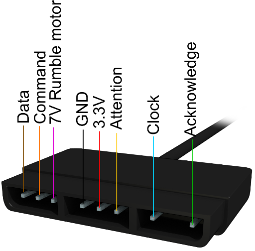
I found more information about the Playstation pinout and interface online.
•
Curiousinventors PS2 interfacing page http://store.curiousinventor.com/PS2
•
McCubbin's site https://gamesx.com/controldata/psxcont/psxcont.htm
•
Scanlime's github gist https://gist.github.com/scanlime/5042071
•
Everything You Have Always Wanted to Know about the Playstation But Were Afraid To Ask by Joshua Walker. http://hitmen.c02.at/files/docs/psx/psx.pdf
•
pinouts.ru https://pinouts.ru/Game/playstation_9_pinout.shtml
•
Near Future Laboratory - PlayStation 2 Logic Analysis http://blog.nearfuturelaboratory.com/2008/06/19/playstation2-logic-analysis/
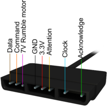
The Playstation pinout indicates that the pad requires two power supplies: one for the logic and one for the motors. I found differing sources indicating that the logic supply can be anywhere from 3.3V to 5V or above. However, it seems to be commonly found that the consoles themselves supply 3.3V for the logic and 7.6V for the motors.
The protocol itself is a SPI-compatible protocol, which is very considerate of Sony. I've used SPI before in the
Ocelot Arcade System to control a
TLV5618A 2-channel DAC reet-quick, so I know what it's all about. Specifically, it seems like it resembles Framed SPI. More on this specific later!
In the Playstation controller protocol, SPI is used to exchange 8-bit messages with the controller. This protocol is simultaneous duplex, controlled and clocked by the console. While the console is sending a command message out, the controller is sending data back to the system. Since the controller can't know what the system is asking for until the message has been received, the first response will be a garbage byte. After that, the controller is able to respond to the messages it has received up to this point. since hte console is controlling the rate and number of transmissions, the console must execute the correct number of exchanges in order to receive the full response to any request it makes to the controller.
A typical exchange with an original PS1 digital controller or an analogue controller in digital mode looks like this:
| Playstation | 0x01 | 0x42 | 0xFF | 0xFF | 0xFF |
| Controller | 0xFF | 0x41 | 0x5A | data | data |
•
0x01 is an attention message to begin an exchange. The controller idles its response data line which is read as
0xFF.
•
0x42 polls the controller for its button state. Meanwhile the controller responds to
0x01 with
0x41 indicating its controller type and data length in 16-bit words.
•
0x00 0x00 0x00 are dummy messages to allow the controller to respond to the request.
•
0x5A is a spacer message used when the controller is not ready to respond yet.
• The controller responds to
0x42 with two
data messages holding the button state response bitfields.
The console stores the responses to its messages and extracts the appropriate values and bitfields. Read the documents for more info!
 It's an Amiga 1200, magically transmuted into the form of a video game console. It has two 9-pin controller ports on the side, which are the same as those found on the Amiga home computer series (but not the CDTV, even though it's an A500, though Commodore pretended it wasn't). As such, it's compatible with all Amiga controllers, such as the magnificent, clicky, and magnificently clicky Zipstik joystick, and two button pads like the Sega Master System. However, since it's a nifty video games machine, it has its own special, completely-incompatible-with-everything-else, controller. That odd, telephone/dogbone looking thing, there.
 Replacement directional pad design by Ndo Design. https://www.shapeways.com/product/XLKEBL3WQ/commodore-amiga-cd32-controller-d-pad
It's a disc shape with protruding fingers on its base to lock it into a notched circular holder inside the pad. With minimal use (and thirty years of age) the notches can break, freeing the disc to rotate underneath your thumb, which moves the cardinal direction studs and contacts underneath out of position, making the pad nearly unusable.
That's no good, especially if you just want to be a lion.
I looked up possible ways to fix the pad, along with schematics for it. I wondered how difficult it would be to build a new pad from scratch completely - which didn't seem to be particularly difficult as it consists of eleven contacts and two standard logic chips. Designing and 3D printing a new pad case or D pad was possible, even plausible, but a little beyond what I felt like doing at this point.
I hadn't done any microcontroller work in a while and also wondered if I could simulate the function of those chips in software. Since Playstation pads and their cheap-but-effective clones are still being manufactured by the million to this day (2019), a Playstation to CD32 convertor was the natural choice.
The first thing to do is to research absolutely everything.
• How does a CD32 power a CD32 controller (if it needs to)?
• How does a CD32 console talk to a CD32 controller?
• How does a Playstation power a Playstation pad?
• Can a CD32 power a Playstation pad?
• How does a Playstation console talk to a Playstation pad?
• Can a CD32 power a Playstation pad together with some guys that translates the messages?
The CD32 stuff
Replacement directional pad design by Ndo Design. https://www.shapeways.com/product/XLKEBL3WQ/commodore-amiga-cd32-controller-d-pad
It's a disc shape with protruding fingers on its base to lock it into a notched circular holder inside the pad. With minimal use (and thirty years of age) the notches can break, freeing the disc to rotate underneath your thumb, which moves the cardinal direction studs and contacts underneath out of position, making the pad nearly unusable.
That's no good, especially if you just want to be a lion.
I looked up possible ways to fix the pad, along with schematics for it. I wondered how difficult it would be to build a new pad from scratch completely - which didn't seem to be particularly difficult as it consists of eleven contacts and two standard logic chips. Designing and 3D printing a new pad case or D pad was possible, even plausible, but a little beyond what I felt like doing at this point.
I hadn't done any microcontroller work in a while and also wondered if I could simulate the function of those chips in software. Since Playstation pads and their cheap-but-effective clones are still being manufactured by the million to this day (2019), a Playstation to CD32 convertor was the natural choice.
The first thing to do is to research absolutely everything.
• How does a CD32 power a CD32 controller (if it needs to)?
• How does a CD32 console talk to a CD32 controller?
• How does a Playstation power a Playstation pad?
• Can a CD32 power a Playstation pad?
• How does a Playstation console talk to a Playstation pad?
• Can a CD32 power a Playstation pad together with some guys that translates the messages?
The CD32 stuff
 The first two questions were answered by searching for schematics and pinouts of a CD32 pad online. I could have (and should have) taken my own one apart to see if I could fix the broken directional pad at the same time, but having bits of irreplaceable plastic raining down on my lap would've just depressed me.
Here's a mirror of Gerd Kautzmann's CD32 controller page. (http://gerdkautzmann.de/cd32gamepad/cd32gamepad.html)
Oddly enough it seems to exist because Gerd was frustrated that the directional pad was on the left side of the pad, which didn't suit their grip, rather than the thing being an unresponsive, fragile, irreplaceable pile of tat.
They have a wonderful, if needlessly confusing, schematic of the pad:
The first two questions were answered by searching for schematics and pinouts of a CD32 pad online. I could have (and should have) taken my own one apart to see if I could fix the broken directional pad at the same time, but having bits of irreplaceable plastic raining down on my lap would've just depressed me.
Here's a mirror of Gerd Kautzmann's CD32 controller page. (http://gerdkautzmann.de/cd32gamepad/cd32gamepad.html)
Oddly enough it seems to exist because Gerd was frustrated that the directional pad was on the left side of the pad, which didn't suit their grip, rather than the thing being an unresponsive, fragile, irreplaceable pile of tat.
They have a wonderful, if needlessly confusing, schematic of the pad:
 This pinout from the KTRL CD32 project is a definitive CD32 pinout:
 The mechanics of the CD32 can be mystifying at first, but I've got to master them if I want to create a device that speaks the same protocol.
For example, in isolation, this is meaningless:
The mechanics of the CD32 can be mystifying at first, but I've got to master them if I want to create a device that speaks the same protocol.
For example, in isolation, this is meaningless:
 This somewhat-combed spaghetti shows a few things:
• The two joystick ports are identical.
• The box labelled RP401 is a resistor array that pulls all the directional input pins up.
• The directional inputs are read using a uni-directional 74157 multiplexer so the Amiga can't set any pin high or low to change the behaviour from the described.
• The three Fire inputs link internally to points labelled _FIRE0, POT0Y and POT0X within the Amiga chipset.
_FIRE* links to a CIA on an A500 (Akiko on a CD32), and POT** link to Paula in both an A500 and a CD32. (The POT** pins are used for two axes of analogue input on each joystick port, for paddles and pens and other inventions.) Functionally, this means that all three can act as general purpose bidirectional IO pins, and can be configured as output low (sinking current), output high (sourcing current) or High-Z (no effect on output voltage, reading value from external effects), and can be read during any of these settings.
This means that with some fiddling magic, the Amiga can actively perform a protocol to read values from the controller.
Here's the pad schematic again:
This somewhat-combed spaghetti shows a few things:
• The two joystick ports are identical.
• The box labelled RP401 is a resistor array that pulls all the directional input pins up.
• The directional inputs are read using a uni-directional 74157 multiplexer so the Amiga can't set any pin high or low to change the behaviour from the described.
• The three Fire inputs link internally to points labelled _FIRE0, POT0Y and POT0X within the Amiga chipset.
_FIRE* links to a CIA on an A500 (Akiko on a CD32), and POT** link to Paula in both an A500 and a CD32. (The POT** pins are used for two axes of analogue input on each joystick port, for paddles and pens and other inventions.) Functionally, this means that all three can act as general purpose bidirectional IO pins, and can be configured as output low (sinking current), output high (sourcing current) or High-Z (no effect on output voltage, reading value from external effects), and can be read during any of these settings.
This means that with some fiddling magic, the Amiga can actively perform a protocol to read values from the controller.
Here's the pad schematic again:
 First, I'll define a table of pin names and roles:
 • The Amiga can now read the value of the Blue button at pin 9 DATAOUT.
• On the rising edge of pin 6 CLOCKIN (controlled by the Amiga), the value at pin 9 DATAOUT will change to the next input, which is Red.
• On each new rising edge of pin 6 CLOCKIN, the next input will be presented, in this order: Blue, Red, Yellow, Green, FF, Rew, Pause, 1, 0, 0, 0...
The sequence of inputs returned can be seen on the schematic as pins H through A on the shift register, with the SER shift-in input being used to provide an endless sequence of zeroes (Lows) once the eight variables have been exhausted.
This means that:
• If the JOYMODE pin is set low, the pad is set to seven button shift register mode. On the falling edge of the JOYMODE signal, the states of the Blue, Red, Yellow, Green, FF, Rew and Pause buttons are captured, and the state of the Blue button is presented on FIRE2OUT/DATAOUT. FIRE1OUT/CLOCKIN is treated as an input signal. On each rising edge of FIRE1OUT/CLOCKIN, a new button state is shifted onto the FIRE2OUT/DATAOUT line in a set sequence. When all seven buttons have been shifted, a final 1 signal is reported, followed by endless 0s.
In both modes JOYMODEs, the Up, Down, Left and Right inputs are exactly the same as those of a dumb joystick.
To summarise:
• The CD32 pad has two modes, determined by the state of the pin 6 JOYMODE pin. This pin is controlled by the Amiga, and is one of the three bidirectional pins the Amiga joyport has.
• If the JOYMODE pin is set High by the Amiga, the pad is set to a dumb joystick mode. The states of Fire 1 (Red) and Fire 2 (Blue) are reported to the Amiga by grounding the FIRE1OUT and FIRE2OUT pins respectively as if Fire 1 and Fire 2 were simple switches to ground.
• If the JOYMODE pin is set Low, the pad is set to seven button mode. CLOCKIN is treated as an input signal. On each rising edge of CLOCKIN, a new button state is shifted onto the DATAOUT line in a set sequence. When all seven buttons have been shifted, a final 1 signal is reported, followed by endless 0s.
Notice that the FIRE1OUT/CLOCKIN pin is bidirectional in this protocol, and its role changes based on JOYMODE. Specifically, it is an output if JOYMODE is high, and an input if JOYMODE is low. Because the Amiga can change the state of pins 5, 6 and 9 on each joyport at any time, and because the system runs arbitrary game/program code directly with no hypervisor or hardware locks, the states of these pins are able to change at any time. This means it very possible and likely for a device plugged into the joyport to cause bus contention, with both the device and the Amiga attempting to drive one of these pins at the same time if it doesn't react properly. This is Not Good.
I asked on the English Amiga Board for information about the electrical characteristics of the Amiga's joystick ports. They supply 5 volts through a 4.7 ohm resistor. Good to know.
Phew!
So any device I design will have to have the above behaviour, and do it safely in such a way that it doesn't self-destruct, kill the Amiga it draws power from or kill the controller it powers.
The Playstation stuff
• The Amiga can now read the value of the Blue button at pin 9 DATAOUT.
• On the rising edge of pin 6 CLOCKIN (controlled by the Amiga), the value at pin 9 DATAOUT will change to the next input, which is Red.
• On each new rising edge of pin 6 CLOCKIN, the next input will be presented, in this order: Blue, Red, Yellow, Green, FF, Rew, Pause, 1, 0, 0, 0...
The sequence of inputs returned can be seen on the schematic as pins H through A on the shift register, with the SER shift-in input being used to provide an endless sequence of zeroes (Lows) once the eight variables have been exhausted.
This means that:
• If the JOYMODE pin is set low, the pad is set to seven button shift register mode. On the falling edge of the JOYMODE signal, the states of the Blue, Red, Yellow, Green, FF, Rew and Pause buttons are captured, and the state of the Blue button is presented on FIRE2OUT/DATAOUT. FIRE1OUT/CLOCKIN is treated as an input signal. On each rising edge of FIRE1OUT/CLOCKIN, a new button state is shifted onto the FIRE2OUT/DATAOUT line in a set sequence. When all seven buttons have been shifted, a final 1 signal is reported, followed by endless 0s.
In both modes JOYMODEs, the Up, Down, Left and Right inputs are exactly the same as those of a dumb joystick.
To summarise:
• The CD32 pad has two modes, determined by the state of the pin 6 JOYMODE pin. This pin is controlled by the Amiga, and is one of the three bidirectional pins the Amiga joyport has.
• If the JOYMODE pin is set High by the Amiga, the pad is set to a dumb joystick mode. The states of Fire 1 (Red) and Fire 2 (Blue) are reported to the Amiga by grounding the FIRE1OUT and FIRE2OUT pins respectively as if Fire 1 and Fire 2 were simple switches to ground.
• If the JOYMODE pin is set Low, the pad is set to seven button mode. CLOCKIN is treated as an input signal. On each rising edge of CLOCKIN, a new button state is shifted onto the DATAOUT line in a set sequence. When all seven buttons have been shifted, a final 1 signal is reported, followed by endless 0s.
Notice that the FIRE1OUT/CLOCKIN pin is bidirectional in this protocol, and its role changes based on JOYMODE. Specifically, it is an output if JOYMODE is high, and an input if JOYMODE is low. Because the Amiga can change the state of pins 5, 6 and 9 on each joyport at any time, and because the system runs arbitrary game/program code directly with no hypervisor or hardware locks, the states of these pins are able to change at any time. This means it very possible and likely for a device plugged into the joyport to cause bus contention, with both the device and the Amiga attempting to drive one of these pins at the same time if it doesn't react properly. This is Not Good.
I asked on the English Amiga Board for information about the electrical characteristics of the Amiga's joystick ports. They supply 5 volts through a 4.7 ohm resistor. Good to know.
Phew!
So any device I design will have to have the above behaviour, and do it safely in such a way that it doesn't self-destruct, kill the Amiga it draws power from or kill the controller it powers.
The Playstation stuff
 Now we can consider the Playstation side.
For the question of how much power the Playstation 2 pad draws, I asked on the Electrical Engineering Stackexchange. I got one comment saying 'do an experiment'. Several weeks later, the question was deleted. You're great, lads. I guess questions nobody immediately knows the answer to make you look bad, huh?
Google didn't help much either.
Now we can consider the Playstation side.
For the question of how much power the Playstation 2 pad draws, I asked on the Electrical Engineering Stackexchange. I got one comment saying 'do an experiment'. Several weeks later, the question was deleted. You're great, lads. I guess questions nobody immediately knows the answer to make you look bad, huh?
Google didn't help much either.
 I found more information about the Playstation pinout and interface online.
• Curiousinventors PS2 interfacing page http://store.curiousinventor.com/PS2
• McCubbin's site https://gamesx.com/controldata/psxcont/psxcont.htm
• Scanlime's github gist https://gist.github.com/scanlime/5042071
• Everything You Have Always Wanted to Know about the Playstation But Were Afraid To Ask by Joshua Walker. http://hitmen.c02.at/files/docs/psx/psx.pdf
• pinouts.ru https://pinouts.ru/Game/playstation_9_pinout.shtml
• Near Future Laboratory - PlayStation 2 Logic Analysis http://blog.nearfuturelaboratory.com/2008/06/19/playstation2-logic-analysis/
The Playstation pinout indicates that the pad requires two power supplies: one for the logic and one for the motors. I found differing sources indicating that the logic supply can be anywhere from 3.3V to 5V or above. However, it seems to be commonly found that the consoles themselves supply 3.3V for the logic and 7.6V for the motors.
I found more information about the Playstation pinout and interface online.
• Curiousinventors PS2 interfacing page http://store.curiousinventor.com/PS2
• McCubbin's site https://gamesx.com/controldata/psxcont/psxcont.htm
• Scanlime's github gist https://gist.github.com/scanlime/5042071
• Everything You Have Always Wanted to Know about the Playstation But Were Afraid To Ask by Joshua Walker. http://hitmen.c02.at/files/docs/psx/psx.pdf
• pinouts.ru https://pinouts.ru/Game/playstation_9_pinout.shtml
• Near Future Laboratory - PlayStation 2 Logic Analysis http://blog.nearfuturelaboratory.com/2008/06/19/playstation2-logic-analysis/
The Playstation pinout indicates that the pad requires two power supplies: one for the logic and one for the motors. I found differing sources indicating that the logic supply can be anywhere from 3.3V to 5V or above. However, it seems to be commonly found that the consoles themselves supply 3.3V for the logic and 7.6V for the motors.
 The protocol itself is a SPI-compatible protocol, which is very considerate of Sony. I've used SPI before in the Ocelot Arcade System to control a TLV5618A 2-channel DAC reet-quick, so I know what it's all about. Specifically, it seems like it resembles Framed SPI. More on this specific later!
In the Playstation controller protocol, SPI is used to exchange 8-bit messages with the controller. This protocol is simultaneous duplex, controlled and clocked by the console. While the console is sending a command message out, the controller is sending data back to the system. Since the controller can't know what the system is asking for until the message has been received, the first response will be a garbage byte. After that, the controller is able to respond to the messages it has received up to this point. since hte console is controlling the rate and number of transmissions, the console must execute the correct number of exchanges in order to receive the full response to any request it makes to the controller.
A typical exchange with an original PS1 digital controller or an analogue controller in digital mode looks like this:
The protocol itself is a SPI-compatible protocol, which is very considerate of Sony. I've used SPI before in the Ocelot Arcade System to control a TLV5618A 2-channel DAC reet-quick, so I know what it's all about. Specifically, it seems like it resembles Framed SPI. More on this specific later!
In the Playstation controller protocol, SPI is used to exchange 8-bit messages with the controller. This protocol is simultaneous duplex, controlled and clocked by the console. While the console is sending a command message out, the controller is sending data back to the system. Since the controller can't know what the system is asking for until the message has been received, the first response will be a garbage byte. After that, the controller is able to respond to the messages it has received up to this point. since hte console is controlling the rate and number of transmissions, the console must execute the correct number of exchanges in order to receive the full response to any request it makes to the controller.
A typical exchange with an original PS1 digital controller or an analogue controller in digital mode looks like this: