Back to Game Raccoon index...

Matt's Chronoblogical Misadventures In Game Raccoon Land - January 2020

Starting in mid-October of 2019, I designed, laid out, routed, ordered and programmed an SD card based rewritable Mega Drive cartridge called the Game Raccoon! This page is a more (mis)informative journey through the various variations the Game Raccoon went through before the first of its many final forms. If you'd like some more concrete notes about the Game Raccoon Revision 0, read the Technical Report here. Let me begin by saying I'm in debted to everyone who's written books, websites or random messages on forums with information in that I've read, used or dismissed. Only by sharing our knowledge, taking risks, and generally being dudes when everything goes right or wrong will the art advance!

Background

When I was doing bugfixes or possibly doing case design for the PSCD32, my brother asked me what my next project could be now that I'd finished a PS2 joystick adapter. I'd downloaded a bunch of documents about the Nintendo 64 controller protocol, and I was thinking of making a "PSN64" that could be used as a substitute for the N64 pad and its analogue stick that turns to gravel through use. While I was researching how I'd do savegames (since the Nintendo 64 Memory Pak connects into the controller and would have to be emulated or provided for), I resigned myself to the conclusion that non-volatile memory components (like FeRAM/F-RAM/FRAM) compatible with my favoured PIC microcontrollers would be very expensive outside of the surface mount form factor. (Battery-backed save RAM? In 2019? Get real.) My usual approach of finding a supplier that would send me a through-hole parallel FRAM sample component for free didn't work out. Since a design based around surface mount components was looking like a necessity, and I was very happy with the bare PSCD32 boards they manufactured, I got very interested in the surface mount manufacturing capabilities offered by JLCPCB. They have a small catalogue of pieces they supply, which at least simplifies selecting parts for a board. When I was looking up memory types looking for FRAM, I saw that they supply large-capacity parallel interface Flash memory ICs in sizes from 16 megabit to 8 gigabit. I suggested to my brother that, with what I knew, I could probably make something similar to a multi-game Sega Mega Drive cartridge with multiple images installed side-by-side on the same Flash PROM, or a cartridge that contains a single game and plugs into a reprogramming cradle to have its contents altered, and he asked me why I couldn't do a full SD-card-based cartridge with a menu instead. I thought and I thought and I thought and I couldn't think of any reason why I couldn't. Here's a simplified model of the Mega Drive cartridge interface: And I say 'simplified', but there's not really much more to it than that. There's a big mask ROM with a 16-bit wide data bus, and the Mega Drive asks it for numbers at certain addresses and so it spits them out at the appropriate times. The three signals I've highlighted, B16 !OE, B17 !CE and B20 !DTACK, are used to request data and respond to the request. The Mega Drive wants your cartridge to be silent on the data bus until it receives a read signal within the address region assigned to the cartridge. Although the address bus can be decoded to produce the necessary enables, the Mega Drive chipset provides signals !OE and !CE matching the standard Chip Select and Output Enable signals required by almost all RAM and ROM ICs as a convenience. If you wire up like to like, and add a decade pair of capacitors to stabilise the power, you've created a valid Mega Drive cart. In December 2013, I did just that!

The MegaBoard

Like the Master System, the Mega Drive uses 5V power and signalling, so I could re-use the 28C256 chips I'd ordered for my Master System rewritable cartridge for Gravity Beam: Master Gaiden. The MegaBoard uses two 28C256 electrically erasable 8-bit EEPROM chips side by side to provide a 64 kbyte, 16-bit wide interface that's protocol and voltage compatible with the Mega Drive's cartridge port. That photo on the right is the MegaBoard running MD Music Demo 1 by Gigasoft. There aren't many pieces of software that fit onto the MegaBoard, but it plays the 64 kbyte Uwol: The Quest For Money wonderfully! While it's possible to prise the EEPROMs out of the MegaBoard to rewrite them, it's really annoying. Plus I kept forgetting which order the two half-ROMs needed to be inserted into the two bays - since each chip provides 8 bits of the 16-bit response to a request, the original binary image needs to be split into alternating halves. In the present day, I looked up levered sockets to simplify ROM replacement, but they're really big and wouldn't fit in the existing unpopulated MegaBoard boards I have. (Which are yours if you'd like to buy them.) The third signal, !DTACK, is a signal required by the 68000 processor to indicate that a data request has been filled successfully. Until the signal is pulled low by a peripheral, the 68000 will wait. However, for the regions of the memory map assigned to the cartridge, the Mega Drive chipset provides this for you, meaning you don't have to supply it yourself, but placing an implicit minimum speed on the response of the cartridge. If your ROM isn't fast enough, the 68000 will receive the automatic !DTACK from the chipset and whizz off with garbage values. Unless you're making a special device to respond to accesses outside the automatically handled range, you need to leave this signal alone. The routing on this board is a bit frightening, looking back. I just let the autorouter do its thing until it came up with an acceptable answer. The reason it's so tall and blank is to allow the socketed EEPROMs to sit outside of the raised dome of the Mega Drive Model 1. If you're wondering about the name... well it's because it's a board for the Mega Drive. And... I was really bored.

Anyway, let's talk about my new board instead

I've got a whole load of options for how my new board could work. The first step in designing anything is to figure out what it is you want it to do!

Let's start with some constraints:

• The cartridge has to physically fit into a UK PAL Model 1 Sega Mega Drive, since that's what I've got. • The cartridge has to have some kind of on board memory that can be reprogrammed somehow. • The cartridge has to have enough non-volatile memory to do something useful. • The cartridge has to identify itself as, and respond in the same manner as, a normal PAL region Sega Mega Drive cartridge. It's also important to have some facts about Mega Drive games: • They have a 64 pin, 0.1 inch pitch edge connector. There are 32 B pins, running from left to right across the connector on the side that faces the player. There are 32 A pins, running from left to right on the reverse side. Pin A1 is directly behind B1 and so on. That means if you turn the cartridge around in your hands to look at the non-component side, A1 will be on your right. • All 23 bits of the 68000 address bus A1-A23 are available to the cartridge to decode. The address bus pins don't correspond to the numbering of the pins on the A side of the cartridge. The address bus line A0 does not exist on a 68000 since all accesses are word-aligned. To read a byte, the CPU reads the containing word and reacts only to the required byte. • The cartridge outputs only on the data bus, and then only during a read request directed at the cartridge. If this behaviour is faulty, either a valid read request will not be satisfied and garbage data will be read, resulting in a 68000 crash, or spurious read requests will be detected and there will be contention on the data bus as two sources attempt to drive it, resulting in a 68000 crash in the best case, and permanent damage to the Mega Drive motherboard, cartridge PCB, or power supply in the worst case. • We don't need to worry about !DTACK. What we really need is a good source for the Mega Drive cartridge pinout. Unfortunately, at the time, there was no one single good source for this. There are several sources, but they don't agree, and some don't make sense when combined with others. https://melaircraft.net/2019/01/17/sega-megadrive-genesis-cartridge-pinout/ http://www.hardwarebook.info/Mega_Drive_Cartridge https://wiki.megadrive.org/index.php?title=315-5308 https://wiki.megadrive.org/index.php?title=Connectors As you gather more variations, you'll find contradictions, names reused for different purposes, and inconsistent definitions of 'input' and 'output'. The best thing to do is to ask for advice. Or perhaps find examples of working hardware and work from there. If you've got the goodies, you can make your own scans of the Mega Drive bus during operation and see for yourself what each kind of communication looks like. I could only work from these docs though. :) Here's some retail carts - you can see six connections for the address bus on B4-B9, a pair of connections: B16 !OE and B17 !CE, and four connections B22-B25 for the data bus.

First go

First things first, before I thought about technical anything, I wrote down what I'd want the cart to do at the highest level: At this point I'm still thinking about using Static RAM to store the game image, which means that there's also got to be some other non-volatile storage somewhere to boot into, which I've labelled as CART ROM. There's something listed as BRAIN that's going to read from the SD card and put a list of games 'somewhere' so the Mega Drive can read and display it. I don't think at any point I considered an 'online' kind of communication back and forth between the Mega Drive and the BRAIN, only big transactional operations. Writing it down, it quickly becomes obvious that the cart is going to have to be able to isolate itself from the Mega Drive if it's going to write to the SRAM, unless it's dual ported. That's gonna be a mess. At least SRAM is cheap: https://www.digikey.com/product-detail/en/alliance-memory-inc/AS1C2M16P-70BIN/1450-1477-ND/9825432 $2.99 for 32mbit of SRAM. I need 2 megawords of 16-bit wide RAM. This is pseudo SRAM, which has the same interface as SRAM but works internally physically as DRAM with its own integrated refresh circuitry. There's absolutely no way I can solder a BGA (Ball Grid Array) package though. Down in the bottom left I've made a note saying the bootstrap ROM has to be at least 1kbyte - a pretty bold bid that I'll be able to fit the 68000 exception table, Mega Drive header, and all the operations and graphics I need to perform the menu in 1kbyte. I think I was just listing the minimum ROM space to get anything at all on-screen. Here's another crack at the sequence of operations. It'll power on, pass the TMSS check (that's the password you need in order for software on the Mega Drive to run - spoilers: it's SEGA), copy the bootstrap ROM to RAM and then execute from there. It's a good plan. (And I should know since it's the approach I went with in the end two months later for Revision 0. :D) What's next on this page though is the suggestion that I treat the MCU as a memory mapped peripheral and send it commands directly to query the SD card and populate the title listing and so on. That's not something that an MCU can really do directly, since it's not fast enough. If you want a programmable part that works natively as if it were a logic component, and at those speeds, that's CPLD and FPGA territory as far as I know. What follows is a bunch of scribbles wondering what kind of logic gates would be needed to provide a memory map on the cartridge to put the bootstrap ROM and MCU in separate logical locations. I'm still thinking about manually decoding the A22 and A23 address bits here to enable the SRAM block for when a game is ready to launch. Down in the lower right, I've identified a need for a dedicated line to select between the bootstrap ROM and the SRAM since they'll both have to be present at the same location in the Mega Drive's memory map, since they're both going to perform the task of simulating a normal mask ROM cartridge in the range $000000-onwards. I need to transmit commands and the index of the selected game to the MCU somehow. At this point, I'm thinking about using a SPI channel to do it, since it'll be fast enough to acknowledge 68000 bus signals. If I generate the SPI clock with logic based on the signals coming out the Mega Drive during a read operation, I could send data to the new board one bit at a time for sure. In the second page on the lower right I've made an observation about !DTACK that isn't quite right, but was consistent with what I knew at the time. In a 68000-based system, peripherals need to respond on !DTACK to indicate that a read operation has completed. Simple systems have a grounded !DTACK, which means that all read operations are presumed to have finished within the earliest window they could have. In reality, the Mega Drive chipset provides its own predetermined !DTACK for certain address ranges, including the cartridge, but not in others, which allowed them to design new peripherals (like the Mega CD and 32X) which could signal their readiness at their own speed. Here's another attempt at the control flow from the board to the Mega Drive. There doesn't seem to be any indication of bus isolation here; the MCU and the SRAM and the Mega Drive would all be active together at the same time, communicating amongst themselves using specific addresses and signals - it hasn't yet coalesced into a sensible method yet. I'm firmly stuck on the idea of a simple linear list of games at this point. Also at the top I've written that I need to look into whether I need to work with the Mega Drive's own reset signals. The board would work without it, coming alive and reset when the power was applied, as would the SRAM, but its state would remain unchanged if the player hit the Reset button, which would definitely cause a huge mess on the bus when the Mega Drive tries to boot from the cart while it's busy doing MCU things.

Organisation, a.k.a. Drawing Lots of Rectangles

I've succumbed to the temptation to draw lots of rectangles and feel like a super genius. There's so many components going on here... SRAM at the top for the temporary game storage. Logic chips and latches running down the left side, selecting devices and storing state signals that the MCU writes into them for the 68000 to read from later. The bootstrap ROM is listed as being one 16-bit data bus piece or two 8-bit data bus pieces. Sensible. There's a line flying all over the place labelled D0. I don't think I'd fully thought through the approach with that line yet. It very definitely comes in handy later, but its purpose isn't listed on this page... This is the first appearance of the 3.3V regulator, which is very necessary for this project. The 28C256s in the MegaBoard were 5V, but it's no longer vogue to manufacture devices that run from a 5V supply. SRAM ICs, MCUs and logic run from 3.3V, though they may be tolerant of 5V inputs - which means they can accept the signals from 5V devices without blowing up, but they'll still only output 3.3V high. db-electronics seems pretty adamant I get the voltage issues right! I've also listed the PICKIT, since I was really hoping to not have to buy a whole new programmer for this one project. This would make the third project I'd used my PICKIT 2 on, after the Ocelot and the PSCD32. It's a useful gizmo. This restricts me to the set of devices programmable by a PICKIT 2. And that's a bit of a funny story. I asked on the Electronics Stack Exchange for a list of devices compatible with the PICKIT 2. My question was voted up, received several answers, one of which provided a useful Wayback link to a now-deleted page on the Microchip website containing the information I needed, which I accepted. Then the question was closed for being off-topic. For being a direct, answerable, useful question about a specific device that is only useful in an electronic engineering and hardware design context? I'm afraid I'm just not smart enough to get it. Those diagrams on the right are the read and write timing diagrams for the 68000 as listed in Microprocessor Systems Design by Alan Clements. It's a wonderful book that I'm very glad to have picked up for next to nothing from Oxfam several years ago. I've finally addressed the huge elephant in the room: that the Mega Drive and the MCU need exclusive access to the internal buses of the cartridge if they're going to be taking turns using the SRAM for different purposes. That means tristate buffers! Here, I'm considering manual decoding of the address bus to create an enable signal that will pass through GPIO signal values from the MCU through the cart edge to the 68000, effectively turning the combination into a memory mapped peripheral (which I've named MCU GPIO DBUS here) from the 68000's perspective. The pull-up I drew is probably not necessary, since the logic gate is always going to be outputting something... but it won't be if the power hasn't stabilised! Here's some more manual address decoding. Below the line I'm constructing my own !CE and !OE signals using !AS, following the timing diagrams in the book: if the address is the one you want, and the address is stable, pull the enable low. I'm using the R/!W directionality signal from the 68000 here. The !CE I create is then going to be used as an input to further logic to select either the bootstrap or SRAM devices. I could've saved myself a bit of money had I stopped myself here, but I worked with what I knew, and what I knew was consistent. And it worked! Anyway, I'll talk about what I mean later. I'm envisaging a BUSY signal on the MCU here, and there's a lot of thinking going on as to what order things will happen. I'm picking out some parts to make the cartridge from, setting some constraints. I'm using Sega Retro's database of game sizes to figure out whether I'm likely to encounter any software that would use the full 4 megabyte addressable cartridge space. The freely downloadable game Wiz 'n' Liz is 1 megabyte, and Zero Tolerance is 2 megabyte. I'd be very happy to be able to run either of them on the cartridge. I have a friend in the demogroup TiTAN who wrote a demo called Overdrive for the Mega Drive. Overdrive is 4 megabytes big, so makes sense to just go ahead and make the cartridge's SRAM the full proper size. On the right I've identified a possibility for the transceiver that I'll need to use in order to provide a 5V to 3.3V pathway for signals coming into the cartridge and 3.3V to 5V for signals emitted by the cartridge... I'm listing the ROM size of some PICs at the bottom since they'll need to store the SD card library and the program for writing to SRAM. The $A130xx region is special, I read - various flashcarts use it for communication. Hadn't realised quite why yet. :) Interesting things to come! This is looking a lot more promising now that the bidirectional transceivers are in place. There was no way the cart was going to work (safely and reliably) without level translation or the ability to isolate the internal cartridge buses from the Mega Drive. Making the selects for the 164245. Collectively these transceivers and selection rules conceptually group all the modules on the cartridge into one composite device with similar semantics to an un-accompanied mask ROM: it's 'silent' (outputting nothing on the data bus) until it receives a request to read from the part of the address to which the cartridge has been assigned. This is a bit of an aside observation, but it might save me some time or effort later on. Although the pins are labelled D0-D15 in the datasheets of the PROM and RAM, all that matters is that the data is read out using the same permutation of pins. A similar observation applies for the address bus, with the caveat that the bootstrap ROM uses a smaller subset of address pins, so care needs to be taken. The PIC, if it connects to the bootstrap ROM and SRAM, is going to be entirely GPIO driven, so I have control over the pin mapping. Also I can't believe I wrote 'EEPROM burner' here, as if I'd have a huge 28C256-type fellow on the board somewhere. This is clearly getting way too complicated. There's over a dozen things on the board, 23-pin buses with four endpoints...

"ALL GAMES ON ONE CART... CART!"

As an exercise, knowing what I've worked out so far, I've had a stab at figuring out how things like this surely authentic "Newest 196 in 1 Sega Genesis Mega Drive 16 bit Multi Cart Cartridge" would work. I also like how the compatibility advice on the second image is listed as 'Warm Tips'. Not quite as crucial as a hot tip, but certainly not room temperature. Behold, the organisation diagram for the 'ALL GAMES ON ONE CART... CART' Hypothetically, if you tried to install all 700+ Mega Drive games into one device, you'd need at least 700 * 4 megabytes, assuming every game gets its own dedicated 4 megabyte address space, and we ignore games bigger than 4 megabyte (which is... one). That's 2.8 gigabytes. Let's throw away some games and round it down to 512 games and 2 gigabytes. 2 gigabytes (16 gigabits) of Flash memory is nothing at all, though it would be hard to get it in a 16-bit wide data bus form. Now we have a device with the lowest address bits A0-A20 selecting words from a single given 4 megabyte game slot (4 megabytes = 2 megawords = 2 ** 21, so 21 address lines used), and the upper bits A21-onwards forming a number selecting which game slot to use. If we attach a latch to these pins, we have a stable number that we can change at any time with a signal. Now all that's needed is a way to put a value into the latch to select the slot, and a stable boot process that presents what the Mega Drive expects. On boot, you could use a self-resetting latch (like the 74LVT16373A), or use the Mega Drive's reset to reset it. With the latch on zero, the zero slot will be presented to the Mega Drive, making it the implicit boot partition. To put a value into the latch, set up some address decoding (or not, if you're feeling courageous) to detect a write to your device, and route the data bus into the inputs of the latch. The Mega Drive will have to be executing from RAM at this point since otherwise the currently running routine would vanish as soon as the contents of the latch changed and the new slot was prevented. So the boot partition will have to copy itself to the Mega Drive's RAM first before doing any bank prestidigitation. How you do target the latch from the Mega Drive? The !TIME signal plays a big part in other folks' custom Mega Drive cartridges, and, reading this far, they must be jumping about in their seats wondering why I haven't tried to use it yet. So here it is. In the Mega Drive's chipset, !TIME refers to the address range $A13000-$A130FF. This address range appears to have been assigned for use by any cartridge-based peripherals. The name 'TIME' I'm told refers to its primary intended use as real time clock support. For flashcarts and the like, the TIME region is used for communicating with the on-board magic, though games and peripherals are free to use it however they like. Sonic 3 uses the signal !TIME it as part of its bankswitching without decoding any part of the address value - it's used as the CLK input to a D-type latch with D0 as the data input (according to the schematic by Krzysiobal). In the second image, I'm considering combining !TIME with other address signals to produce a selection signal for the slot select latch. If I use !TIME alone, then the latch will respond to all !TIME accesses, which would cause games to malfunction if they try to access it and cause themselves to be bankswitched into oblivion. With a more specific selector, my latch is placed at a more restricted address subrange of my choosing. So: The boot partition starts, shows your predefined menu, and when you're ready you can jump to RAM, swap to a new slot, then launch that slot as if it were a cartridge. The components are all standard and cheap, and everything is super reliable. Adding in the correct level shifting and directionality and enable logic is important unless you ensure globally 5V-tolerant parts and are confident your Mega Drive works off 3.3V signalling. That's a good plan. Cheap, simple. That must be why they do it! But I don't want to do that. I'm going back to the static-RAM-based cartridge, and figure out how it would work with the parts in JLCPCB's library: The IS62WV51216BLL mentioned in the top right is 1 megabyte (8 megabit) of static RAM, as 512 kwords of 16-bit. This is the largest 16-bit parallel static RAM I could find in JLCPCB's parts catalogue which was in stock. JLCPCB doesn't support BGA, which means that the 32 megabit PSRAM from before is out of reach. There's a few non-parallel static RAMs, which are of absolutely no use here. Using four 1 megabyte SRAM units becomes very complicated very quickly: The SN74LVC138ANSR is a fast 3.3V 3-to-8 decoder that takes a 3 binary digit input number and outputs eight individual active-low enable lines, allowing the designer to select one of eight devices based a value such an address or latched number. I'm trying to figure out how I can use this decoder to enable multiple SRAM chips and a non-volatile bootstrap ROM correctly. Tables and diagrams galore! I'm thinking of the speed of the logic used here: the LVC series has the fastest speed, which is very important for something that will be in constant, frequent use. I'll be using a lot of LVC later on. :) This specific decoder also has three extra global enables that all need to be satisfied simultaneously for any of the outputs to be active-lowed. These allow the decoder to itself decode part of an address to detect whether the part of the address range that it's responsible for is being accessed. I'm working out which of the Mega Drive's signal lines I'd need to pass through and level translate. In the oval is the 74ALVC164256DL,118, a dual-supply 5V and 3.3V dual-octal transceiver that acts as a pair of 8-bit bidirectional buses with individual enable and direction control signals. This is the transceiver that I need to use in order to provide a 5V to 3.3V pathway for signals coming into the cartridge and 3.3V to 5V for signals emitted by the cartridge. The 164245 is the logic number; different manufacturers will decorate it to represent the manufacturer and implementation family such as ALVC. I'm seeing this model of transceiver on a lot of other modern cartridges, so it seems like the way to go! How you'd get anything onto a non-volatile module in the first place, whether it contains games or a bootstrap ROM, is a conundrum. You'd have to either program it before you attach it to the board, or program it with some header pin array that exposes the Flash IC's pins to an outside programmer. Or if you were feeling very swish, make an external cart programmer with a Mega-Drive-compatible slot that your new cart plugs into for programming. For me, programming it before assembly is not going to happen - as cheap and as interesting the concept is, it's not something I'd be able to make by hand. Surface mount really does rule the world, which really sucks for hobbyists. Let's get rid of the SRAM altogether. Having an array of chips running across the cartridge together with a non-volatile boot ROM would've been horrific.

Let's simplify it.

How about we replace the SRAM array with a single Flash chip. Now we have two Flash chips: a 4mbyte one for the game to be written into, and a smaller one for the bootstrap ROM. Using the Flash as a rewritable ROM gives us different characteristics than using SRAM, but it will still work. These will still have to programmed and all the rest. There will have to be logic to select between the two devices, distinguishing between the boot and game Flash units. This is starting to sound a lot like the 'All Games On One Cart' cart, but with only two slots. When you think of it like that, there's no reason why they have to be distinct devices at all! Consider a single 8 megabyte capacity, 16-bit wide Flash module. That's twice as big as the address space allocated to the Mega Drive mask ROM cartridge, just like the multi-game cartridge concept, except with only two slots. Slot zero must be the bootstrap ROM once again, and slot one will be a 4 megabyte rewritable region which can store a single game. Now the role of the SRAM and the non-volatile storage is combined into a single device. With an MCU like a PIC on-board the cartridge responsible for the programming, we can dedicate some GPIOs for controlling the bidirectional transceivers, as well as satisfy the role of the slot selection latch using a pin as a !BOOT/GAME signal, which will be 0 when the boot ROM is active, and 1 when the game half of the Flash is active. When the cartridge is powered up, the MCU have all its pins as high-impedance inputs until its firmware chooses otherwise, so this pin will need to be pulled to ground to provide a stable default of 0 on power-on. 64 megabit, 16-bit wide Flash modules are cheap and common - the SST39VF6401B-70-4I-EKE in the JLCPCB parts library is one such part. This is looking a lot more doable already! How would that look in terms of organisation? With the SRAMs and latch gone, things are way more straightforward. Since the Flash module is the only device that responds to read signals, and it will respond to the full 2 megaword address range the Mega Drive will attempt to read from, the Flash can just be linked up to the first 21 lines of the (post-transceiver) address bus. (Noting again that 2 ** 21 is 2 megaunits - i.e. 2 megawords addressable.) In this design, the PIC will be responsible for writing boot ROM and game images to the Flash module, reading game images from the on-board SD card socket, as well as controlling all the stateful control signalling within the cartridge. I've picked out the PIC24FJ64GA006 since that's compatible with my PICKIT 2, and it's in the JLCPCB parts library. The tiny text on the diagram a calculation of how many pins the design will need of whatever MCU I use: it'll be connected to the 16 pins of the internal data bus, the 22 pins of the internal address bus (including the !BOOT ROM/GAME selector, the 4-pin SPI SD card interface, the 2-pin PICKIT interface and whatever state pins I need. I suppose I ought to define what I mean by 'isolation' here. :)

Defining what I mean by 'isolation' here

When a Mega Drive cartridge is connected to a horizontal slot on the Mega Drive motherboard, it's as if you'd soldered it into the motherboard directly onto its address, data and signals buses: it'll see all the signals traded between the 68000 and the VDP, and the 68000 and the RAM. The cartridge has to remain idle until it's specifically asked to respond. My design now has internal address and data buses of its own connecting the Flash module and the PIC. These buses allow the PIC to write values into the Flash, which is how it will install game images. However, for this to take place, it needs exclusive access to both the address and data buses. Other than playing dangerous games with !DTACK, there's no simple way for the cartridge to request the buses all to itself from the 68000. My solution is to use the transceivers as both voltage translators and a conditional barrier between the 68000 world and the internal board world. The directionality and enable of this barrier will be controlled by select signals derived from the signals on the Mega Drive's signals bus, but with an added flag which will immediately disable all the transceivers, isolating the board from the Mega Drive. This flag named !68000 will be controlled by the MCU, and will be low when normal communication between the board and the Mega Drive is in effect: that is it will attempt to emulate a normal mask ROM cartridge, and will be high when isolation is required. Since the MCU will power up with its GPIO pins in a high-impedance state, it will be pulled low by default with a resistor. When isolation is in effect (this phrase will recur a lot throughout the document), the internal address and data buses will float, and the post-transceiver manifestations of the Mega Drive's signals bus will need to be pulled to default states by resistors. I'm still considering manually decoding !CE from the higher address bits here, on the left. The note underneath on the sketch explains that during isolation the address bus will be floating, so the A22 and A23 pins used to construct the CE condition will have to be pulled low. At the bottom are transceivers translating and isolating the cartridge's internal address and data bus from those of the Mega Drive. The !AS, R/!W and !TIME signals will have to come into the cartridge somehow to detect read and write conditions. Experimental engineering! • I wanna do X • Hmm, but I can't do X like this • But if I could do X it'd look like Y • Sketch out an X using Y • Y is very complicated, but a Z that performs the role of Y would be simpler • Z is better than X in some respects! • So lets try Z!

A small reality check

Now that I have some idea what parts I might be using, a reality check is in order. For each part I'm going to install on the board, I need to look up their worst-case current draw during full activity and add them together (possibly with some fudge percentage added) to get a worst-case current draw for the cartridge as a composite device. If this is greater than the safe current supply of the Mega Drive's cartridge slot, then something has to give. Determining the safe current limit of the Mega Drive port is something that I suppose would have to be determined by some very risky wizards through trial and error. A useful starting point would be find or make a passthrough cartridge extender that would allow you to interpose an ammeter in the 5V supply path to determine the typical current draw of a normal retail cartridge of the era. This would almost certainly be miniscule, however, since real cartridges for the most part have no computational elements in them. I'm not liking that 100mA for the SD card. I don't know where I got that from. I'm not sure if it's burst current or power on or what. I've identified the AMS1117-3.3 as a possible regulator for the board: a simple, small linear regulator to take the supplied 5V and transform it into 3.3V. Don't forget to look in the datasheet for the details of the required surrounding support capacitors. This fellow wants a tantalum capacitor on its output terminals. The PICs of the Ocelot and the PSCD32 both required one of these too, and they're annoying to get from smaller shops since they're not ordinary electrolytic or ceramic capacitors. They're not especially unusual or expensive, but they can be when you have to order them special from Farnell when the rest of the parts come from the mom-and-pop shop.

Communication between Mega Drive and board

Communication between the Mega Drive and the new board needs to be figured out. The Mega Drive needs some way to send values to the PIC that it can decode as instructions/codes/symbols to progress through the cartridge state flow from boot -> menu -> install game -> select game -> boot game, and vice versa to report state and results, as well as report the contents of the current directory. Certain PICs have a Parallel Master and Parallel Slave modes, allowing the PIC to (as I understand it) imitate a latch and receive or send parallel values. This sort of sounds like it would be useful for this project, but I haven't the foggiest how they work. Every time I look them up, they seem to be a useless imitation of what I want them to do, so I just ignore them. Trying to get the PIC to act like a latch using GPIOs and interrupts is way too slow: if the Mega Drive writes to the PIC using a normal memory access cycle, the PIC would have to handle the interrupt and slurp up the relevant ports within the small window while the data was available. This is what !DTACK is designed to handle, but now things are getting more complicated again... What would be best is a configuration where the Mega Drive can throw a value out at the cartridge at the normal speed, and the PIC could then awaken, isolate the cartridge and then retrieve it at its own pace: a 16-bit temporary storage zone for values yet to be transferred. That's a latch, right?

About the Flash

Speaking of writes, timing, and interfaces, let's look through the Flash module's datasheet for a moment. I don't want write protection, so I'm pulling !WP high. Correctly !RSTing the Flash when the Mega Drive starts sounds like a good thing. I'm not sure entirely how much state there is inside the Flash to reset though... The only other signals left to consider on the Flash are !CE, !OE and !WE. !CE is a global enable for all the chip's functions. It must be asserted low for either !OE or !WE to have any effect. The Flash module has the same interface as RAM or ROM does for word-wide random read access, but writing to the Flash is completely different from SRAM. The Flash module acts like a self-contained system in itself. I wouldn't be surprised if there's a simple microcontroller inside the package controlling everything (which is kinda zany, considering things like SD cards are Flash memory modules coupled with a controlling microcontroller...). The Flash's memory space is split into discrete sectors that must be first be erased before they can be written to. Once erased, the bytes can be programmed randomly, or quickly programmed in sequence. These operations are wrapped as complex commands that are submitted through the data bus and clocked in through !WE. The datasheet lists special constant sequences (reminds me of port knocking) that trigger various commands within the Flash. I'm going to have to see which of the Flash's commands my system will use, and implement these within the PIC's firmware as a driver library.

More organisation

Here's what the system looks like now with the latch. Pretty good! These signals coming out of the address transceiver ought to be pulled up to force them idle when the cartridge is isolated. The control signals to the various devices shouldn't be though, since they'll be the output of gates. The MCU's outputs have to have defaults though, since they'll boot up as floating! On the right I'm noting that I don't need to install the latch like a T on the data bus since the D and Q pins are directly opposite one another physically, so I can place it on top of the data bus. That gives me the modified form of the diagram shown in small in the middle right where the data bus runs underneath the PIC's communication latch. I'm glad I'm not jumping into this and blowing loads of money on getting it made. I'm like a really boring snooker player on my twentieth chalk. The audience leans over the advertising panels in anticipation whenever I lay my palm on the baize, and I take the cue in hand and do that uncomfortable looking thing where the movement rubs their chin, and then I get up again and chalk the cue some more. There's a few inches of bright blue dust covering the floor with my shoeprints in circles around the table.

Glue logic

Determining the glue logic that combines the Flash, PIC, transceivers and latch together! Here I'm laying out the pieces that I have to work with: the inputs that the Mega Drive will give me, and the outputs that I'm trying to control on the cartridge. I'm using !TIME to identify when the Mega Drive is accessing the latch, but still decoding A23 and A22 to detect cartridge access. Controlling the directionality and enable of the three transceivers is paramount. If this is wrong, the Mega Drive will blow up instantly. Not really an exaggeration. Here I'm listing three transceivers: address, signals and data. The cartridge never tries to output an address onto the Mega Drive's bus so that direction is a constant. Same for the signals. The data transceiver direction depends on whether the Mega Drive is writing or reading. The enables of the transceivers depends on the cart's isolation state and what kind of operation the Mega Drive is trying to perform. The action of the data transceiver has to exactly match the function that a normal cart's combined devices (mask ROM and SRAM) would perform. For ROM reads: data comes from the cartridge onto the Mega Drive's data bus. For latch writes: data comes the Mega Drive and onto the cartridge's internal data bus. For all other conditions, the data bus is high-impedance. With that information in hand, I can design the cartridge's state flow from booting to gameplay:

Cartridge state flow from booting to gameplay

I'm going to need to write smaller. Alright! I'm going to transcribe this for you:
68000MCU
POWER ON MEGADRIVE INACTIVE !VRES LOW FOR 16.7ms MCU+FLASH HELD IN RESET STATE ADDRESS 5V-->3.3V SIGNALS 5V-->3.3V DATA 5V X 3.3V !68000 PULLED LOW !BOOT/GAME PULLED LOW !WE FLASH PULLED HIGH !OE LATCH PULLED HIGH
!VRES NEGATED
STANDARD MEGADRIVE BOOTSEQUENCE CART CHECKSUM + SEGA READ FROM BOOT SIDE OF FLASH BOOTS FROM ENTRY POINT OF BOOT ROM BOOT ROM: SELF TEST? COPY TO MEGADRIVE RAM JUMP TO MEGADRIVE RAM SHOW/SETUP SOME STATUS/WELCOME MESSAGE SIGNAL TO CART TO BEGIN - WRITE VALUE TO !TIME - - - -> MCU BOOTS, SET PIN STATES FOR A+D BUSES SPI1 SETUP BUT NOT EXECUTE !68000 OUTPUT LOW !BOOT/GAME OUTPUT LOW !WE FLASH OUTPUT HIGH !OE LATCH OUTPUT HIGH MCU BUSY/LOW POWER UNTIL EDGE DETECTED ON LOAD LATCH
NOP FOR A SHORT DURATION ATTEMPT TO READ 0x000004 THIS IS THE ENTRY POINT OF THE CART SPACE ROM. IF IT IS ODD (D0=1) THEN THE ISOLATE IS IN EFFECT AND THE CART IS BUSY. ELSE THE ISOLATE IS COMPLETE, AND THE TITLE TABLE IS READY. test_for_isolation: move.w $000004,D0 (this should be .l) andi.w #$0001,D0 bne test_for_isolationNOP FOR A SHORT DURATION READ LATCH: SET ISOLATE ON, PULL !68000 HIGH [ SET DATA BUS TO INPUT [ SET !OELATCH TO LOW [ STORE DATA BUS TO VARIABLE [ SET !OELATCH TO HIGH [ SWIZZLE DATA BUS VALUE? (BRANCH ON VALUE) PERFORM SEQUENCE FOR 32KWORD BLOCK ERASE FOR TITLE TABLE SPACE BEGIN SDCARD COMMS READ AND SORT ROOT DIRECTORY LISTING (SORT MAY BE DONE ON MEGADRIVE SIDE?) WRITE TITLE TABLE TO FLASH (STORE NO. ITEMS OR RELY ON $FF FLASH ERASED STATE?) CONTINUE UNTIL ALL TITLE TABLE IS WRITTEN (NAME, SIZE) WHEN DONE, DISABLE SDCARD.
; ISOLATION NO LONGER IN EFFECT TITLE TABLE IS AVAILABLE READ/SORT TITLE TABLE, MAINTAIN LINK TO ORIGINAL ORDERING AS THIS IS THEIR SDCARD POSITION. TEST TO SEE IF TITLE TABLE IS VALID? SHOW FANCY MENU WITH TITLES,MUSIC,SFX,SPRITES ETC. USER SELECTS A TITLE FROM THE LIST. WRITE SDCARD INDEX NUMBER TO !TIME - - - - - ->RECONNECT TO 68000 BUS: !68000 LOW BUSY/LOW POWER UNTIL EDGE TRIGGERED ON LOAD LATCH
NOP FOR A SHORT DURATION SHOW FUNNY DISTRACTING ANIMATIONREAD LATCH: SET ISOLATE ON, AS ABOVE !68000 LOW (SWIZZLE?) TO GET ID OF GAME SELECTED ENABLE SD CARD, OPEN INDICATED FILE DETERMINE WORDS TO WRITE DETERMINE MINIMUM BLOCKS TO ERASE SET !BOOT/GAME OUTPUT HIGH FOR BLOCK = 0 TO WRITEBLOCKS-1: [ READ+WRITE MIN(BLOCKSIZE, WORDSREMAINING) WORDS [ WORDSREMAINING -= MIN(BLOCKSIZE, WORDSREMAINING) [ IF WORDSREMAINING == 0 BREAK GAME HAS BEEN WRITTEN TO GAME FLASH FLASH IS SET TO PRESENT GAME HALF OF ADDRESS SPACE DEACTIVATE SD CARD
USE ISOLATION TEST TO SEE IF GAME WRITING IS COMPLETE. <- - - ON COMPLETE: move.l $000004,A0 jmp (A0) JUMP TO ENTRY POINT OF GAME ROM, AS MCU HAS TOGGLED !BOOT/GAME HIGH BEFORE DISABLING ISOLATION. GAME ROM IMAGE IS NOW IN CONTROL. CART ACTS AS 4mByte DUMB ROM SOURCE IN GAME ADDRESS SPACE OF FLASH.SET !68000 OUTPUT LOW TO RECONNECT CART BUSES MCU LOWPOWER/INFINITE LOOP DO NOT RESPOND TO !TIME OR LATCH EVENTS.
DONE.DONE.
• The boot ROM boots first, since it has to, and transfers control to the PIC once it has copied itself to RAM. • The PIC populates a 'title table' stored in the Flash PROM on the boot side somewhere with the names and sizes of all the games on the cartridge. This means that all the games are going to be stored in the root for now. • When the title table is complete, the cart deisolates and the boot ROM in RAM can display the menu. • The user picks a game from the list, and this index is written to the PIC and the boot ROM sleeps. • The PIC reads the index and writes the appropriate game to the game partition of Flash, deisolates, then sleeps forever. • The boot ROM in RAM awakens and jumps to the game. It couldn't get any simpler. It might actually work! :D There's a sneaky trick in here that I haven't yet described which is pivotal to the back-and-forth between the Mega Drive and the cartridge.

A sneaky trick

I wrote: ATTEMPT TO READ 0x000004 THIS IS THE ENTRY POINT OF THE CART SPACE ROM. IF IT IS ODD (D0=1) THEN THE ISOLATE IS IN EFFECT AND THE CART IS BUSY. To allow the Mega Drive to determine whether isolation is currently active or not, a pull-up resistor is attached to the D0 signal on the Mega Drive-facing data bus causing the least significant bit of any word to be read as a 1 if no other device is driving the data bus. In the Mega Drive ROM header, which all games are required to adhere to in order to boot on the system, the least significant bit of a longword or word value is known to be 0 at many fixed locations in a valid game ROM image: specifically, anywhere where a word-aligned address value is stored, such as the stack pointer initial value stored in longword $000000 and the cartridge entry point address stored in longword $000004. With a valid Mega Drive ROM installed in the active Flash partition, longword reads from $000000 (or word reads from $000002) must have D0 == 0 when a valid ROM is available, i.e. when the cartridge is not isolated. The addition of a pull-up resistor on the Mega Drive-facing side (making sure to connect it to 5V, not the regulated internal 3.3V) will force D0 == 1 when the cartridge is isolated and unable to respond to the memory read. If the Mega Drive already contains a pull-up or pull-down resistor on D0 to stabilise the value, then my approach won't work unless my resistor is stiffer than the one on the motherboard. I think that's pretty clever, if it works. That's put me in the mood to get out some squared paper and see what's what.

What's what on the PIC24FJxxGA006

Here's a diagram of the GPIO pins and relevant preallocated peripheral pins on the PIC24FJxxGA006. At the bottom is a pinout of an SD card in SPI mode. The pins MOSI, MISO, CLK and !SS are all that's needed to connect an SD card to a PIC it seems. Whoever laid out this PIC is a bonafide lunatic. There's 64 pins on the chip, 11 of them are used for power, so there's 53 left for comms. In C, the GPIO pin states are mapped to variables, and an int is 16-bits, so there's a variable called PORTA which you can read or write to set or get the values on the corresponding GPIO pins. Except there's no A on this chip, it starts at B and goes up to G. The only port that has all 16 pins present is B, and I can't use all of them because it overlaps with some of the debugger pins. All the other ports have holes in their assignments and are assigned out of order around the edge of the chip. There's no way to wire up a series of 16 related inputs to a single port and read their values into a single variable with a single instruction, unless you use a specific pair of debugger pins and wire everything up in twisty ways. If you wire things up to ports in contiguous ways and do it in a way that actually reduces the number of instructions necessary to retrieve and present values (instead of a way that you think reduces them), then you can trade preparation time before the device is manufactured for execution time when the device exists.

Registering what a Latch isn't

I've been looking through all the 74 logic datasheets that I can find, and I don't think a latch is what I want at all. The logic of a latch's LOAD line is similar but inverse to what I want - that is, it's 'transparently open for loading' when its control line is high, and frozen in state when the line is low (I think?). What I want is the device to act as a single word of memory with the same interface any RAM: data to be stored is presented on the D inputs of the register, and a rising edge to the register's CLK stores the value. The register outputs its current stored value on the Q outputs when its !OE is asserted low. Such an instrument is the Turbo Encabulator SN74LVC16374 16-Bit Edge-Triggered D-Type Flip-Flop With 3-State Outputs. The register (D-type flip-flop) action is important here because it matches the 68000 write cycle, so it can be added to the board without any fuss. If I connect the D and Q buses together, the register now has the action of recording and replaying a single 16-bit value it has seen on demand. The register CLK will have the same polarity and timing as a corresponding 'strobe' signal would have, so I can use the following expression to create a clock signal that will write the current data bus value into the register when the Mega Drive attempts to write to any !TIME address: REGISTERCLK = !TIME + !AS + R/!W Finding out the difference between a latch, register, and flip-flop ain't easy. Hope this helps! A latch remembers whatever value was in it while you hold it open, like somebody looking through a doorway and remembering it. And while the thing on the other side of the door changes, the memory changes constantly. And when you close the door it remembers what was last visible. A register is more like a photograph. Its memory stays the same constantly until its clock goes 'ping', and then whatever the state was at that moment in time is its new memory, a lot like writing to a variable in a programming language. I'm gathering a fearsome collection of truth expressions now. I wish I had some easy way to verify them.

Making Truth Tables

Well, I couldn't find one. There's no decent boolean truth table generators on the Internet? I find it difficult to believe, but disbelief didn't help me find one, so I wrote one. This truth table generator is written in JavaScript and lets you enter expressions, one per line, with any number or complexity of inputs. Outputs can be reused as inputs on subsequent lines. Anything that isn't an output is an input and will be automatically toggled for you to produce the full truth table. Here are the expressions I have so far: FLASH!OE = MCU!FLASHOE*(SIGNAL!C_CE+SIGNAL!AS+NOT(SIGNALR/!W)) FLASH!CE = SIGNAL!C_CE ADDRESSTRANSCEIVER!OE=MCU!68000 REGISTERCLK=SIGNAL!AS+SIGNALR/!W+SIGNAL!TIME MCUDETECTREGISTERCLK=SIGNAL!AS+SIGNALR/!W+SIGNAL!TIME DATATRANSCEIVERDIR=SIGNALR/!W DATATRANSCEIVER!OE=MCU!68000+((SIGNAL!C_CE+SIGNAL!AS+NOT(SIGNALR/!W))*(SIGNAL!AS+SIGNALR/!W+SIGNAL!TIME)) Now that I've used this tool, it's time to... never use it. It's way too difficult on the eyes, and trusting the computer to do something that I could do by hand sounds like one way to turn my brain off and make mistakes all over the place.

More organisation

Trying to add the logic for selecting the register and Flash based on the incoming signals makes for a very messy diagram, but it's true to how complex the final physical device will be.

What the Transceivers Should Do

I've noticed that the address and signals buses both have the same directionality and enable conditions: they're both input-to-the-cart only, and they're always active unless isolated by the PIC. This means I can use two transceivers for the address-signals bus instead of dedicating discrete transceivers to the second half of the address bus and the signals bus. For this transceiver, the DIR pin is H if the signal path should 'go Higher': from the lower to the Higher voltage. Conversely, the DIR pin is L if the signal path should 'go Lower': from the higher to the Lower voltage.

Getting close to good logic

Time for another complete attempt at the logic. It's the 25th of October now, and I was musing in my secret blog about 'The cheapest way to interface the Flash, the MCU, the Register and the Transceivers.' and combined these together to come up with the possible cart name 'FMCURT'. I'm... uh... kinda glad I didn't call it that. The incoming !C_CE, pulled low during isolation, goes to the Flash's !CE pin. A request by the Mega Drive to access the Flash ROM is determined by !AS + NOT(R/!W) + !C_CE, which goes to the Flash !OE. Except how can the MCU access the Flash now? There needs to be another gate to allow two signal sources to access the Flash, going low if either of them are activated. The register clock will go low when a correct strobe on a !TIME write takes place: !AS + R/!W + !TIME, which the MCU also needs to be able to detect. The data transceiver direction is set by the read/write direction coming from the Mega Drive. The address transceiver output enable will be controlled by the MCU's !68000 output pin, which is pulled low during reset. The data transceiver output enable will be active when a Mega Drive Flash ROM read or Register Write takes place, but not if the bus isolation is active. That's not a three input OR gate though... the result of that OR gate would always be HIGH because one of the mutually exclusive 'Mega Drive ROM read' or 'Mega Drive Register write' signals would always be high, making that construction meaningless and useless. Try again. The incoming !C_CE, pulled low during isolation, goes to the Flash's !CE pin. A request by the Mega Drive to access the Flash ROM is determined by !AS + NOT(R/!W) + !C_CE, which goes to a gate which pulls the Flash !OE low if this signal is received or the MCU's !FLASHOE is set low to force the Flash to output. The register clock will go low when a correct strobe on a !TIME write takes place: !AS + R/!W + !TIME, which the MCU also needs to be able to detect. The data transceiver direction is set by the read/write direction coming from the Mega Drive. The address transceiver output enable will be controlled by the MCU's !68000 output pin, which is pulled low during reset. The data transceiver output enable will be active when a Mega Drive Flash ROM read or Register Write takes place, using an AND gate. The MCU can override this with its own HIGH signal on !68000 if isolation is in effect.

Second opinions

Since the last time I'd done anything for the Mega Drive was six years ago, I decided to get a second opinion on my concept and logical design before I went any further. In fact, I hedged my bets and got three second opinions from the EEV Blog forum, Spritesmind and Obscure Gamers! One of the suggestions I got was to eliminate the PIC and replace it with a CH376 File Manage And Control Chip. This chip abstracts SD card access, USB mass storage access, FAT16, FAT32, and FAT12 filesystems and presents simple parallel I/O, serial or SPI interfaces. It does Everything, it seems! And it's $2.82. That's somewhat pricey in device terms as far as I know, but if it does all the things that's claimed of it then that's a lot of problems solved. And it is a JLCPCB Basic part. The reason I'm not going to consider it is that it doesn't solve any problem that I have, and introduces new problems I can't solve. Consider a layout like this: In this layout, the Mega Drive is the one that writes to the Flash, so the control section must be set up to allow writes to be directed there. I've mapped the CH376 into the Mega Drive's address space as a parallel I/O device, probably into !TIME; taking over the whole region. Isolation is no longer needed, as long as the control section can ensure that the Flash and CH376 only respond to correctly addressed requests. The control section also now has to take on the responsibilities the PIC had in holding state for !BOOT/GAME. The sequence for this CH376-based system works like this: • System powers on, control section !BOOT/GAME is reset. • Mega Drive boots from boot partition. • Boot partition contains stub that copies itself to RAM. • RAM-resident menu communicates through !TIME to CH376 and gets SD card contents listing. • RAM-resident menu lets player browse through directories, and finally select a game. • Mega Drive opens file with CH376 and receives file one byte at a time. • Flag changes Flash to game partition and engages write mode. • For each received word, write word to Flash - erasing sectors as well as needed. • File is closed. • When 'boot game' option is chosen, jump to entry point on ROM. This sounds acceptable in theory, but my instinct says the Mega Drive would be really dang slow at shuffling bytes around! Reading and writing 4 megabytes like -this- would be awful: ; erase current sector move.w #32768,d1 program_next_word_within_current_flash_sector: move.b TIME,d0 rol.w #8, d0 move.b TIME,d0 move.w #FLASHCOMMAND_PROGRAM,#FLASHCOMMAND_COMMANDADDR move.w d0,#FLASHCOMMAND_COMMANDADDR dbf d1,program_next_word_within_current_flash_sector Then again, (6 instructions / 1.4 MIPS) = 4.3 microseconds, which is the same order of magnitude as the fastest per-word averaged programming speed of the S29GL064S Flash module: 3.125 microseconds (page 97 of the datasheet), so it wouldn't be a disaster. But... there's no way to get the initial boot ROM onto the cartridge in the first place, which makes this approach useless for me. You'd need a programming cradle that'd act as a Mega-Drive-with-a-special-BIOS that would automatically load a predefined file from the SD card and write it to the boot partition of the Flash. Another suggestion was to not use the S39VF6401B Flash module since the programming is word-only, and requires a slow command 'knock' sequence in order to disable the protection to get the single word inside it. In typical fashion, I misread the advice, responded with a polite comprehensive calculation based on an incorrect assumption on the device's workings, and barrelled on regardless. If you'd like to find how what effect this piece of ignorance on my part had on the functioning of the board, read on!

Choosing physical components

When choosing the physical components that will implement the logic and transceiver operations, it's essential to ensure that they're all electrically compatible! The lowest output-High of all the devices collectively needs to be greater than the maximum input-High of all the devices collectively. The datasheets of the devices you buy will show this, usually in a cryptic table showing the output voltages under different output current conditions. Consider the output current that will be present under each possible condition, and use that: logic that interconnects devices will have very little current draw (or sink) and so the output logic voltages will be very close to their ideals (near the supply rail voltages usually), output pins that are used to power devices will have high current draw (or sink) - when a logic pin or GPIO is used to control an LED, the output voltage will be distorted by the need to power the devices in series with the pin. For my invention, everything seems fine. With the very light, signal-type currents involved, everything will output highs near 3.3, and the highest required threshold for a HIGH is 2V, which is also listed as the VIH value for the 68000 processor in its datasheet. The VIH for the other components on the Mega Drive's motherboard is unknown (to me), however!

GPIO capability and layout

And again, check that the PIC has the necessary GPIO capability. Another idea for a potential name came to mind, on the same train of thought as 'FMCURT': PIC Flash Register Transceiver = 'PICFLART'. No? No. Here's another diagram of the PIC and its GPIO layout. Up at the top is a table showing the GPIO PORT variable availability. As all the non-power, non-system pins can act as GPIO, some of these pins will share their function with the non-remappable modules of the PIC, such as SPI. Since there are a lot of contiguous bits available in ports B, C, D and E, it would be possible to wire the 16 bits of the data bus to D0-D11 and C12-C15, allowing values to be read and written from the ports using shifts and bitmasking operations instead of bit-by-bit construction - especially since the two ports collectively cover the pin numbers zero to fifteen. Similarly, the 21 bits of the address value can be mapped across E0-E7 and B3-B15. Something to be considered when assigning roles to the PIC pins and routing. And there we have it: a full table showing the 64 pins of the PIC24FJ64GA006 and what they'll be connected to. Of course, in the real Revision 0, I didn't use this...

Reality knocks when I check the pinout

You might think that it was odd that I waited this long to draw out my own complete table of the Mega Drive's pinout. And you'd be right. It was very odd to do so, and not very sensible at all. For example, R/!W signal I was expecting to see from the 68000 isn't present on the cartridge port signals bus! If I want to use those semantics in my logic, I need to make my own !R and !W signals using the logic at the bottom of the page: the Mega Drive exposes the !AS strobe for all CPU actions, and the !LDS and !UDS strobes for writes to even and odd byte addresses respectively. The way I detect a write is to sense when either one of these strobes has been asserted. If I substitute this construction using two NANDs (so I can combine them into a single quad-NAND logic chip) into my logic diagram, I get this: Well that's getting more complicated isn't it? One thing I'm not liking is how many gates there are between !LDS and !UDS and DATATRANSCEIVER!OE: two NANDs, a 3-input OR, an AND and an OR. That means when the write strobes are asserted, the first NAND sets !R from low to high, which is then inverted to low by a NAND, which then may maybe the 3-input OR low (which might in turn be two 2-input ORs consecutively!) to signal the beginning of the register write, which goes into the AND to signal the start of an external data access, which then finally has to be combined with the optional override from the MCU to produce the final signal low output. The processing time of a logic gate is listed as its propagation delay, which will vary depending on logic family and function required, as well as the current input voltage since many devices function at a range of supply voltages. These propagation delays are based on specific test scenarios as well - if there's resistances or capacitances on the signal line, then these will slow the propagation of steady logic signals too. In the worst case, it's possible that by the time the final output has been realised, the event has already passed! What's important is that the required input signals all reach a target device intact, in the correct order and within the windows allowed by the device. I'm considering the length of a Flash byte write cycle given the number of sub-operations that have to take place to make it happen: I have to set the address bus value, the data bus value, and strobe the !WE signal each time. It adds up!

TO REDUCE UNNECESSARY ERASE CYCLES

The write cycles of a Flash module are limited. I believe each sector has an independent lifetime. In my case, they're in the region of > 100,000 each, which simplistically means that you can write 100,000 game images to the game partition before a write fails and the Flash is jammed in a faulty half-written state, containing a mangled, unwritten, unbootable game. However, depending on the use of the cartridge, other parts of the Flash might fail first. It's important to reduce the format-erase wear on every part of the Flash as much as possible. There's no page mapping or other filesystem magic present on the Flash module itself - if I want any of that to occur, then I'd have to implement it myself. However, since the cartridges will always be booted reading from the header starting at 0x000000, that location in both partitions will always have to be rewritten when the executable changes, so fancy filesystem things won't help much. 'Cycles are a limited resource! Prevent unnecessary format-write cycles by allowing reuse of already present data.' 'Reduce unnecessary cycles:' • 'On the game half by having a menu item to allow the user to load the current 'installed' game without rewriting it.' • 'On the boot half by only loading the game list from SD and writing to Flash when you specifically ask it to - if you have the same SD card in, with the same games in the same order then the numeric indices are going to be the same and there's no reason to refresh the list. It'll go very weird if you have changed the SD card in the meantime, so don't do that.' The game partition obviously only contains the 4 megabyte game image. 'FLASH boot side stores:' • '0x000000 -> Non volatile permanent boot menu ROM, RAM-installable stubs, font data, graphics etc.' • 'SOMEWHERE -> Last game installed FAT filename and internal cartridge identifier name. This is so menu can tell you the current installed game so you can boot it if you like.' • 'SOMEWHERE -> SD card contents cache. Stores filenames and sizes of all installed games. Lets you send a 16-bit value to MCU to select a game to boot. Directories would be ostentatious.'

Designing a Menu System Under the Clearest of Blue Skies

In very true-to-form, jumping the gun style, here I am thinking about the layout and design of the cartridge's built-in boot ROM game selection menu. It will: • Show a list of games from the SD card contents cache in the boot partition. Since the boot partition will naturally be available to the executing code when the menu is active, there's no trickery needed to read it. • Allow the user to navigate the list of games and select one. This might be the first occurrence of the game selection value protocol using !TIME: • 0xFFFF refresh game list • 0xFFFE boot currently installed game • 0x0000-MAXGAMES install and boot game N I imagine I was influenced by memories of Tetris Attack's menu, as well as the two-pane layout of the Net Yaroze menu - especially since the cartridge will serve a very similar purpose. I already used a cutesy, diagonally-scrolling, looping background in my Allegro-based Dr. Mario clone Dr. Kain back in 2004 or so, but hey it's a very pleasant style!

MIDNIGHT INSIGHTS™

Here's some MIDNIGHT INSIGHTS™ brought to you in a flurry before I went to bed one day. If I copy the full directory structure from the SD card to the boot partition in the Flash, including full names, then the player can navigate the SD card's contents on the pretty Mega Drive-side menu without having to access the SD card any further. And if each directory and file has an index number associated with its full pathname, then I can keep the same 'send a single number to !TIME to select a game to install' semantics as before, despite the directory structure not being flat any more. Also, since I've got some spare pins, it seems like a shame to not use them to control a pair of surface mounted LEDs! Everything needs flashing lights, right? It'll also be invaluable in making sure the PCB and PIC are all playing sensibly while the work-in-progress board is laid out on my desk long before it sees a Mega Drive at all. It depends on what JLCPCB have available... they surely must be one of the Basic parts, right? I still don't have a name for the cartridge at this point (27th October 2019)! See the sketch on the right where it's called 'MATT FLASH'. And also the SD card comes out horizontally on the upper right!

Pull-up resistances, the data bus

I'm calculating the resistance values of the pull-up and pull-down resistors. Too high and they'll be noisy and unreliable. Too low and they'll draw lots of current and be difficult to override. Calculate the current through the resistor by dividing the voltage difference across it by the value. Multiply this by the number of pull-ups on the board to get a total current draw and power usage from just default signal value imposition! I don't know whether to use resistor chip groups or single resistors... I never used chip resistors in the end, the routing got too fiddly for me. The transceivers I'm using have a very annoying pinout which insists on having multiple power and ground pins all over the damned place. I have to route the supplies through them underneath in a lattice-like arrangement on my two-layer board. At the bottom of the page is an annotated physical layout of the Mega Drive's cartridge edge again. I've circled B16 and B17 since I don't want to get them mixed up with the B17 and B18 I'm going to use. (Future me having drunk himself to death at this point...)

Very serious and useful SD card investigations and documents

I found a download for the datasheet of a Sandisk SD card, which came in very handy as you might expect! No guessing, only answers! At the bottom is a diagram of the necessary wiring to use the SD card in SPI mode. It uses the four normal SPI pins that the PIC has, and needs quite a few pull-up resistors too. Here's some trivia that I learned today! Guess what the write protection switch on an SD card does! Doesn't do a dang thing. It's just a little piece of plastic that slides down from position to another. When you put it into a socket, there's a little angled bracket shaped like a hairclip that gets pushed to one side and which closes a switch and lets the computer read the position. It doesn't, for example, stop the card from being written to internally through magic electronic logic, or prevent power from getting to the card, or anything like that. (Not that anybody has used that switch this millennium.) It's just a dumb lump of plastic that anybody can just ignore when writing to the card if they don't care. On a floppy drive it's a different story. The write protect switch on a 3 1/4 inch floppy disk is also a piece of plastic that slides between two positions. When the disk goes into the drive, it slides in laterally and then clicks down a few millimetres. If the switch is in the right position, it pushes on that prong and that's how it can tell. However, it's the responsibility of the drive's integrated electronics to do the writing to the drive; the computer around it can only send requests, so the floppy electronics can say 'no can do, boss'.

Filesystem support for SD cards on PIC

I haven't yet looked into how, precisely, the PIC on the board is going to handle the filesystem on the SD card. I just assumed it would be an easily solved problem and left it until last. • What library? • License? I don't know what license I'll use for the board, the 68000 boot ROM or the PIC firmware (as of writing and uploading the Revision 0 stuff on the other page, I still don't know. I haven't made it at all permissive yet, because I'd like to finish it myself, and the thought of folks running off in circles making malfunctioning cartridges is frustrating and terrifying.) • ROM requirement • RAM requirement - The filesystem library is going to take some ROM space to store the code, of course. It might have some constant RAM usage for some global variables, or it might all be instance-based - only using memory when I require some structure to contain some status about the filesystem or an opened file. On top of that, there'll be some short term RAM usage on the stack during the execution of any function in the library. • PIC compatibility - PIC24FJ64GA006 - 64kB ROM, 8 kB RAM • Select SPI module to use - It would be convenient if the library I use lets me select the SPI module (the PIC I'm using has two) that's to be connected to the SD card. Otherwise, I'll have to route the board and assign the PIC pins according to this constraint. Below that are my choices: • 2018 Latest official Microchip 'Libraries for Applications File I/O Library', supporting LFN, FAT32, XC16 compiler, PIC24F support, Apache 2 licensed, configurable SPI pins. • 2013 Legacy latest Microchip 'Libraries for Applications Microchip MDD Filesystem (MDDFS)', supporting LFN, FAT32, Apache 2 licensed. Older, may work, may not? • <2008 Older versions of MDDFS? • FatFs/PetitFatFs, some random library from the internet. Might work, might not. Permissive, non copyleft license. Ideally I'll be able to download the latest official Microchip one, set some preprocessor flags for it to target my PIC, and it'll work straight away. Of course, as according to one of my favourite quotes: the difference between theory and practice is very small in theory and very large in practice. The smartest thing to do at this point would be to get a real PIC, preferably an exact duplicate of the model I want to use, and set it down onto a breadboard to make a prototype device with an SD card socket and a serial terminal or LCD screen for reporting, and see if I can get a directory listing running on it. I'm not going to do that though since I don't have any of that stuff.

A very serious-looking warning

This is a very serious-looking warning from the mysterious Mr. Dictionary himself there. He's telling me that I shouldn't alter the ordering of the pins leading to the Flash to use the substitutability of the pins on the data bus to simplify the routing. He's yelling that I should be aware that the magic number knocking sequences used to communicate with the Flash for writing need the values present in their correct formats in order to operate... but thinking back as I write this, that's not really the issue at all. All I have to do to work around that is store and send the post-permutation version of the data values. The real issue is that unlike the SRAM, the Flash's address space has a defined logical structure to it - it's split into 32 kiloword sectors, distinguished by their common upper address bits. I can write to arbitrary bytes, but I can't erase arbitrary bytes, only sectors - so it makes sense for the address bus to connected to the PIC in a way that preserves the monotonic ascending sectors and words within a sector. Easiest way to do that is to not play silly buggers and just wire things up like-to-like from the start.

The Final Logic Design

Replacing the consecutive NAND pair with separate AND and NAND gates to produce !R and !W gives us the final logic design for the control section of the board! At the bottom are the default states of all the post-transceiver and MCU outputs. The grid at the bottom shows the locations on the Mega Drive cartridge edge of the control signals I'm going to bring into the cartridge. There's two externally triggered conditions that this logic detects: a read from ROM and a write to !TIME. To detect a read from ROM, we look for the condition where the address is stable, the current address is within the cartridge address space and the current action is a read. FLASH!EXTERNALOE = !AS + !C_CE + (!LDS NAND !UDS) To detect a write to !TIME, we look for the condition where the address is stable, the current address is within the !TIME address space and the current action is a write. This is an active low signal which matches the semantics of the register clock - high when idle, low when data is being inserted, a raising edge stores the data. REGISTERCLK = !AS + !TIME + (!LDS AND !UDS) If either of these external conditions are active (low), we detect that with a gate. !EXTERNAL = FLASH!EXTERNALOE * REGISTERCLK If !EXTERNAL is low, the data transceiver should be active, unless the !68000 override prevents this. DATATRANSCEIVER!OE = !EXTERNAL + !68000 The data transceiver direction is defined by whether a read or write is taking place. For reads from the cartridge, 3.3V -> 5V, this must be High. For writes into the cartridge, 5V -> 3.3V, this must be Low. This is the same behaviour of the !W condition. DATATRANSCEIVERDIR = !W The Flash IC output should be active if either an external access is directed at it, or the MCU is forcing it active. FLASH!OE = MCU!FLASHFORCEOE * FLASH!EXTERNALOE The register only outputs if the MCU wants it to, so this is a direct connection to a GPIO pin. The address and signals transceivers are always 5V -> 3.3V, which is a Low on the transceiver directionality pin. ADDRESSTRANSCEIVERDIR = L The address and signals transceivers will always reproduce the external address and signals bus state into the cartridge, unless suppressed by isolation: ADDRESSTRANSCEIVER!OE = MCU!68000 Trying to lay out the routing for the logic section of the board on paper before opening Eagle is an admirable idea, but it's really too complicated to attempt, especially if I haven't chosen the devices yet and haven't bothered to draw everything to scale. Eagle keeps track of all the things you want to keep track of, and prevents things you don't want to happen from happening. Sure, write down some constraints for yourself on paper and the priorities you'd like to observe, but there's no substitute for laying it out in Eagle and seeing what's plausible and what isn't. One thing these diagrams do is allow me to visualise is the pinout of the various logic devices besides one another. It's easier to fiddle and annotate things on paper than Eagle's layout editor. Choosing orientations and selecting pin assignments wherever there isn't a built-in constraint (multiple identical gates to choose from on a chip, multiple substitutable inputs to any given gate) is both art and science at once.

Selecting components from JLCPCB

This is me selecting components from JLCPCB's library of parts they supply for surface-mount manufacturing. I had to go through each potential device in turn and figure out whether they'd be suitable, compatible with the other components on the board, and whether they'd be worth the price. It's useful to learn some of the more common 74-series logic part numbers, such as 00 for NAND, 08 for AND, 32 for OR, etc. But it's better to have a general idea, and then refer to a guide in case you get it wrong! There are many different families of logic, and I'm not going to list them and their characteristics here because I'd only get them wrong too. I chose LVC for everything (transceivers, register, control section), since it was the fastest (so I could worry less about the propagation times), and worked at the 3.3V supply voltage I'm using for the PIC, Flash and SD card. Most manufacturers will supply chips from other manufacturers' special families so don't worry about being stuck with one. Look up logic selection guides from the likes of Texas Instruments and Nexperia if you'd like to know more. It's important to know the full model name, the supplier part numbers, the single price, the multiple price (if the part can only be ordered in some minimum multiple) and the physical package of each component you want to include. These will all be going on the Bill of Materials when you finish your project. Resistors and capacitors have very cryptic names and model numbers, with the value and tolerance hidden somewhere in the middle. Be careful! It's easy to mix up a 47R and 4.7k part if you're not paying attention, or you misread or miswrite a 3 as a B or an S as a 5.

JLCPCB specifications

Before spending designing the board, contact your supplier and get a list of specifications that your project must follow, including minimum feature sizes, number of layers and so on. If they have a template, consider using it! Here's JLCPCB's page. Also that might be the first scale drawing of the completed cartridge I'd drawn in its entirety! If you'll forgive me for jumping to the present for a moment... The final physical cartridge matches the sketch pretty closely!

Booting up Eagle and trying it for real

I think I've done all I can in terms of preparation... it's time to actually boot up (the free edition of) EAGLE and see what I can do. I've just finished the PSCD32 board, so everything ought to be pretty fresh in my mind. Step 1, draw or find the component templates for all the things I'm dropping onto the board. This includes the board itself, you may be surprised to find! When I did the MegaBoard, I used an Eagle component library by Bruce Tomlin that contained components representing the cartridge edge connector of various retro systems including the Mega Drive. There are templates for PCBs to fit in official Sega shells as well as the larger square EA shells, with the differing screw places, as well as templates with both sets of holes to fit either. I'm going to try GENESIS-SMALL, which will definitely fit inside a normal Sega shell. Here's my first go at a schematic: Notice I've gone for the named net approach instead of routing lines all over the place. Using lines would've been hopeless with this many connectors. Using only nets has the very real risk of failing to connect two device you intend to connect when you make a typo in the name of a net, such as MCU!REGISTROE vs. MCU!REGISTEROE, or simply forget your naming convention, such as MCUFLASH!FORCEOE vs. MCU!FLASHFORCEOE. Always double check every connection, and use the design review tools within Eagle! Also, you should have a strong mental image of how the connections should physically look before you begin the schematic design or layout, so that when you're drawing the signals onto the board, you can immediately notice when a connection is missing or heading in the wrong direction. In this design, pins 1-5 of JP1 in the top middle correspond to pins 1-5 of my PICKIT 2, with an extra sixth pin allowing me to apply 5V power externally, and power the board outside of a Mega Drive. Powering the board without external 5V power would entail operating the dual supply transceivers with only a 3.3V supply connected... not a good plan. I haven't put down the Flash module, register or signal pull-ups/pull-downs yet. The boxes around the lower edge are the random glue logic. I wish they had logic symbols on them, as well as the model numbers. The AND and NAND used to generate !R and !W in the lower middle have an identical appearance. I got the components from https://eagle.componentsearchengine.com, which is exactly what it sounds like, and was invaluable. If you type in a model number, you'll get a whole screenful of redundant results for similar/same devices from many manufacturers. The .zip files they give you contain all kinds of libraries for different CAD programs. I only care about the .lbr files for Eagle, though I keep all the .zips I download just in case. For components that aren't on componentsearchengine.com, they have a very, very handy wizard which can make them for you: you tell it the package of the device you want to componentise, and the website generates a form with a blank pinout for you to fill in. You enter in the names of all the signals and their direction and purpose and it'll produce an .lbr for you. I generated most of the components for my Sega board this way. Whenever you get an .lbr from an external source, make sure that the physical dimensions that appear in Eagle's layout editor match those in the datasheet for the exact package and model of the device you want to place. TSSOP-* is not the same as SSOP-*! I've been on my third or fourth attempt for some devices before finding (or generating) the correct library. Alright, that's a lot of board space taken up already just by the address/signal transceivers. Blimey. And I need three of these guys. I've added the Flash and the register. Look at all those grounds and supplies all over the register! It would be very easy to make a mistake drawing those lines joining the inputs and outputs across the register like that, but I did it so it matches the physical layout I want: the connections running directly straight through underneath the register. On the address transceivers the EDGE nets refer to the A1-based numbering given by the Mega Drive/68000, and the CART nets refer to the A0-based numbering used by the Flash module. This means as the addresses pass through the address transceiver, their indices are reduced by 1. Well that clearly isn't going to work. There's too much junk going on. I have some empty EA-sized shells I'd bought to use with the MegaBoard, so I'm going to replace the edge connector with GENESIS-LARGE. That's a lot better. Though... ugh... The random logic section is an absolutely disgrace, and there's so much wasted space all over the place. There's possibly a more efficient way to lay out the bottom section, but let's think about that when it becomes necessary. I have Eagle's autorouter a shot, and that was an immediate failure. I'm on my own here. I've never done anything this complicated before... JP1 looks weird because I've selected a footprint for a right-angled connector so I can use jumper cables on it out the top of the cartridge, as opposed to perpendicular like on the PSCD32 and Ocelot. I'm going to try to put the random logic section in the gap between the address/signal transceivers and the data transceivers. It'll be messy, but it ought to fit. That fraction of a square centimetre ought to be useful. Considering it logically connects to the transceivers on either side and the PIC above, it makes the most sense there. The only signal that'll be flying all over the place will be the final FLASH!OE generated by combining the PIC's override with the detected ROM read condition, which has to run from the random logic section to the Flash module in the upper left. Not great, probably very noisy... I'm driven by sheer curiosity at this point, drawing lines as best as I can, flipping around pin assignments to try and reduce wasted space. There are 21 lines that have to go from the address transceivers to both the PIC and the Flash modules, and 16 lines that have to go from the data transceiver to the same. I've moved the PIC down a little bit since there's no reason for it to be sticking out from the control section so far like that. Right. There's a word for what we've got here, and it's not a nice one. Can you spot the somewhat glaring mistake I've made in getting this far? I've got the cartridge edge wired up, the address bus wired up, the beginnings of the data bus wired... Where the heck is the SD card socket going to go??

Taking a break and thinking over the SD card socket

Time to take a break and think this over. You know when you do something for too long and you start seeing it everywhere you look? I'm seeing Eagle. Let's think about this SD card socket, then. I've deliberately not looked at other homebrew cartridges up to this point, but I am curious what other folks do for their SD card support. Here's krikzz' Everdrive, or one of the earlier revisions I think? Other (I'm assuming future) revisions of the same cartridge seem to use Micro SD cards, but this one uses a half-length SD card socket whose model number I could really use! It also appears on this one named 'first-sd-based-proto.jpg', so I guess I'm thinking along the right lines here. Searching for 'short SD card socket', 'mini SD card socket', 'half SD card socket' took a good long time. It's easier to find pictures of the sockets than the sockets themselves... they're somewhat easier to find on eBay, which would be fine, I guess, since since they're not in JLCPCB's library I'll be soldering them on myself anyway, but I still need a way to get the footprint of the socket for Eagle. Eventually I found a product page which had a stock number (763-6798) on it, which I could then use to find the correct name and number of the socket! These are "693063020911 - Memory Socket, WR-CRD Series, Memory Socket, 9 Contacts, Copper, Gold Plated Contacts, and here's the WÜRTH ELECTRONIC DATASHEET! There's even a footprint on eagle.componentsearchengine.com, so let's get to it! The data line routing isn't going to be especially pretty with this SD card socket laid out like this: it's possible that I'll have to route some of them underneath the socket. Not an error, but not nice either. I've deleted all that mess that I had going on with the address lines. It was useless. Get rid of it. Get rid of everything. Back to paper.

Orienting the PIC

"Having the address and data bus matching the layout of the port hardware numbering saves processing time but imposes a restriction in the routing of traces on the PCB. If I wire up the buses using the GPIO pins freely I shoulder be able to simplify the routing at the cost of added processing decoding read PORTs and setting TRIS and LAT correctly. Also, I can rotate the PIC to move the preassigned pins to other faces if it makes it more convenient." The PICs I'm familiar with, the dsPIC33FJ128GP802 and the PIC24FJ32GA002, have remappable peripheral pins, so I could move the SPI channels to almost any other position on the PIC. The PIC24FJ64GA006 surprisingly doesn't have that capability despite having more pins and ostensibly the same series. I'm not sure if there's an easy to way to check this other than the downloading the datasheet for a PIC and searching for the word 'remappable'. This table shows what predefined pins will be present at each face of the PIC if I rotate it in 90 degree increments. Having the Flash in the upper left, the SD card and PICKIT header at the top and the data transceiver and register on the right places some constraints on how I should orient the PIC. It's important to keep track of the markings on the physical PIC package when placing it on the board. For the normal orientation with pin 1 on the topmost row of the left side, the signal dot in the upper left of the package. When the PIC is rotated, this rotates too of course. And Microchip don't make this easy! On page 2 they have a diagram with the notch and circle marking in the top left, and the diagram is labelled with text showing the PIC model number running left to right across it. Two-hundred-and-thirty-one pages later, they say 'Oh BTW, the text is written left-to-right when the notch and circle marking are in the lower left'. Why is this important? It's something that (some very lazy) counterfeit chips might get wrong. When looking through the catalogue of an unfamiliar supplier (or, heaven help you, eBay), spotting shaky suppliers early is a good move. I've chosen to turn the PIC 90 degrees to the right (from having the marker in the top left). This puts SPI2, PICKIT header 1 (mislabelled as PGD1/PGD2 instead of PGD1/PGC1) and !MCLR on the top edge and the tantalum capacitor on the right. The other three edges have lots of free GPIO pins. Having these on the bottom isn't so helpful, but I can use those pins for the control logic such as MCUFLASH!FORCEOE which needs to connect to gates in the control section. This means that the text on the PIC ought to be rotated 180-degrees when the board is fully assembled.

Pinning and layout of the Flash module

This shows the pinning of the SST39VF6401B-70-4I-EKE Flash module. The Mega Drive bus is numbered A1 upwards as the 68000 only performs word-aligned accesses, but the Flash's address space is measured in words so the lowest address pin is A0. It's important to write this down to avoid errors. The Flash's !CE signal is taken from the transceiver, and !OE is calculated by logic. Down at the bottom is a labelled model of the Mega Drive's cartridge port. (If only I'd marked B16 !OE, alas!) I've finally seen and made an obvious improvement. The 5V auxiliary power was originally part of the PICKIT header set, but there's absolutely no reason for it to be up there, since it would mean that the 5V power would be running all the way from the top of the board to the regulator, beside the 5V supply pins in the lower right. The more obvious and simpler solution is to have a 2-pin header immediately adjacent to these edge fingers, so the auxiliary power imitates the ordinary power connection. The upper pin header now becomes a normal 5-pin PICKIT header. Running a 3.3V power rail around the edge of the board to the SD card and PICKIT... I'm not sure whether that was a good idea or not. I decided not to do it in the end since it wasted space. The top right of this diagram shows the necessary wiring for the SD card again, with a quad gang 10k chip resistor used for the pull-ups. The pins marked with an asterisk are pulled high. Connecting the Reset signal through the cart is a bit confusing as it connects multiple devices and requires a pull-up of its own, as well as a barrier resistor separating the PICKIT override reset from the cart edge reset. At the bottom you can see the original name of the cartridge: the Megatronic Hyperdrive (also known in the U.S. as the Gentronic Hyperesis).

A new layout with the short form-factor SD card socket

Putting the SD card interface in the top centre frees up the upper right region of the board for routing and swizzling the data bus, but it means there's a lot of traffic in the small space above the PIC and beside the Flash. All the PICKIT programming leads would have to go all the way to the top right, underneath the densely packed data bus. I thought about tucking it above the Flash too but that became very cramped as well. While I'm erasing things, I've redone all the placement and routing on the bottom half of the board. Notice how I've connected the unused inputs on the signal transceiver to ground. Read the datasheets for your components to see what to do with unused inputs on transceivers, gates and so on. Leaving them floating is almost never the correct answer. The new routing has freed up some space above. Eagle doesn't like me routing lines too close to the pairs of screwholes, but there's enough space to run five lines between the larger hole and the edge of the board, so that's a start. I've run power and ground lines up the right side of the board so I can place and link the sockets pull-ups, completing the right side of the cart. The PIC has slid a little to the left since if I wire up the address bus correctly, it shouldn't take up much more space than 21 lines and a bit extra for a via lump or two. I'm really tempted to ditch the PIC's capacitors sticking out in every direction, but the book says they should be there, so they stay.

A FAT library break

My eyes are really going funny, so I'm taking a break and looking through those FAT libraries once more. There's no point having the boards manufactured if I can't get at least one of these libraries to at least compile somehow. I'm making progress with FatFs, since it's consistently recommended on the Microchip forums, though it looks to be written in a kind of twisty, dense C that goes against my own longwinded style. Also, in diskio.c, the word 'result' is consistently misspelled as 'reslut'. Since the project is MIT-style permissively licensed, the code will show up in any other projects' source that have included it... Another strange construction that appears in FatFs is the constant array that stores the number of days in each month named samurai. static const BYTE samurai[12] = {31, 28, 31, 30, 31, 30, 31, 31, 30, 31, 30, 31}; Trying to get the official PIC FAT32 filesystem code to compile... It's complaining about an undefined reference. Somewhere a function is being called after being declared, but no definition is being supplied so it can't link... BUT it's a function that I'm not using, and the line number gcc is giving me doesn't call that function. Something for later.

Layouting out the new layout, carefully

Watch the address bus creep up the board, spreading out to the right once it's reached the Flash. :) I've decided to abandon the idea of having the PIC GPIO-to-bus index assignments be consecutive, and instead I'm assigning pins on the PIC according to where they'd be most convenient to route. Writing to the Flash module will be slightly slower, but the routing is considerably simplified. I'm working on the address lines from the transceiver from left to right, keeping all the vertical connections on the top (red) layer and all the horizontal connections on the lower (blue) layer. As I go along, I'm exposing a via from each trace so that each via will be spaced one via apart, then they can be routed straight horizontally right towards the PIC and linked to the most convenient vacant pin. Being creative but also very cautious with the via placement around the PIC is the only way to route so many parallel pins out of such a small area together. I've routed the data pins straight from the data transceiver to the PIC's vacant right side. Surprisingly, there is enough space south of the SD card socket for all sixteen pins to take a 90 turn to the left! Now that all the data pins are routed, I can separate them out gradually, adding a new via in one-by-one, exposing a row of vias that the right side of the Flash module can reach into on the completely blank blue layer above the PIC. And that's it! I don't think there are any more airwires left!

Reviewing the completed layout

Let's see what the Eagle design review tools say about this hopeless tangle. Surprisingly, not a lot! The constant refining of paths results in a lot of what Eagle calls 'wire stubs'. These are small segments of laid routes that branch off from your main trace in T shapes, but are near invisible since they overlay pads and connectors, and they're really annoying, just on an aesthetic level if anything. Use the Eagle tools to find them and eliminate them. Disconnect sections of traces and redraw them if you have to. I prefer to have my traces running parallel to the length of a surface mount pad than branching from it diagonally. Eagle is warning me about the physical footprint of the Wurth SD card socket: the circular mounting holes are too close to the solder mounting pads on the upper layer. There's nothing much I can do about this. If I buy some of these connectors myself, I'll be able to see if these holes underneath are necessary to fit the piece. If the holes are necessary, then I ought to contact JLCPCB and verify that the resulting design is manufacturable. Tips for Eagle: • Hold Alt to switch to a finer-grained grid snap when placing vias. • Don't use this to place vias closer together than you would ordinarily. Lots of space is good! • Use thick traces for power and ground! I didn't do this (actually I DID, but a change from 8 to 10 in the interface wasn't as much of a leap as I hoped), and it didn't have any bad effects, and I have no idea how exactly I could have done it differently with the density of connections that I have, but I keep getting told to do this, so you do it for me, okay? All that's left to do is neaten it up... AND • Manually verify the logic on paper again. • Select every single net pin in turn and verify by eye that the correct corresponding terminals light up. • Verify that every device has the correct footprint and pinout. • Verify that the Pin 1 markings for each device, where present, indicate the correct orientation for each device. • Verify the edge connector component pin labelling corresponds to the correct Sega Mega Drive pinout. • Verify that I haven't swapped the front (B on the Mega Drive) and back (A on the Mega Drive) accidentally. • Renumber all the components on the board. • Identify the value of each capacitor and resistor. • Identify the correct model number of each capacitor and resistor. • Identify the correct JLCPCB part number of all parts. • Work out how much all the components would cost and the total cost to have it manufactured.

Footprints and logic devices

Looking through the footprints for the logic devices is a nightmare. It seems like there's a dozen different standards for the package sizes, with every manufacturer having their own. One document I found invaluable in sorting out this mess is https://www.nxp.com/docs/en/application-note/AN10161.pdf PicoGate Logic footprints Application Note. This is a document by Philips Semiconductors which compares the footprints of several major small-package logic devices. The important fact I drew from this document is that many of the different logic package identifiers I'd encountered were either identical or identical-within-tolerances. "The 5-pin packages Depending on the vendor, the 5-pin 0.65 mm lead pitch package is known as MO-203, SC70, SC70-5, SC88A, SOT323, SOT353, SSOP-5-P-0.65A or USV. Figure 1 shows the general package outline and a table of the various dimensions. So despite all of the different names used, all of the packages are footprint compatible. For the 5-pin 0.95 mm lead pitch package, much the same can be said. Depending on the vendor, the package is referenced as a SOT753, SC74A, SC59, SOT23, SOT23-5, MO178, TSOP5 and SMV. Figure 2 shows the general package outline for the 0.95 mm pitch package and a table of the various dimensions. Again, it can easily be shown that even though tolerances vary slightly, all of the parts are footprint compatible." SOT-753 and SOT-353 aren't compatible though. They have different dimensions all over. https://www.nxp.com/docs/en/package-information/SOT353.pdf https://www.nxp.com/docs/en/package-information/SOT753.pdf I had to contact JLCPCB and ask them to clarify this one.

Making a logo and naming the cartridge at last!

It's incredible to think that I manually placed every one of those vias! Eagle has a built in component renumbering dialog, which is handy. I renumbered a lot of things manually afterwards to make them suit my understanding of the board and group together identical devices. Let's move those component designators into nicer positions as well. I want to have a silkscreened logo on here, so I need to come with a name for this thing! All the names I'd come up with up to this point were astonishingly terrible. In a flash of inspiration, I went with Game Raccoon because it seemed kinda kitschy and knock-offy in a Game Genie kind of way, and I could have an animation of a cute raccoon rummaging through a box when it scans the SD card or installs games. Okay, I want it to look hand-drawn. A scribbly bit. The word Raccoon has got to be prominent. Boom. This font is Komika Jam, but I don't like how thin it is. Let's try again. This font is Snaphand by Inkyotter Design, and with a slight alteration to the N to make it smoother on the lower right, I think we have a winner! I could even make a series! Game Raccoon Mega Drive! Game Raccoon SNES! And have a cute logo on the cart as well! I might even ditch the game part and just call it 'Raccoon'. Also this logo is copyright Mathew Carr 2019. The distinctive logo design and the words 'Game Raccoon' are trade marks. :) To add a custom logo onto a board in Eagle, you need to run the import-bmp script using, well, run import-bmp as described here: https://learn.sparkfun.com/tutorials/importing-custom-images-into-eagle/method-3-import-bmp. You will need to convert your logo into a two-colour 8-bit .bmp first - a retro game graphics tool like Usenti is good for this since there may be fiddly palette manipulations involved. The import-bmp process creates a new library component representing the logo, which can be placed onto your board like any other part. The component contains the logo on one of the silkscreen layers. Remember you'll need to select the correct layer when following the steps in the script. (Eek, an image from the future!) If you want the logo to appear on the reverse of the board, remember that Eagle's default view is to view and modify all layers of the board in X-ray-style vision from top to bottom: text and logos on the bottom silkscreen and copper layer may need to be manually mirrored horizontally. I don't really have one big empty area on the board for a Game Raccoon logo, though, just the upper middle area beneath the PICKIT header, and the area to the right of the PIC. Bingo! It's a little small, but it's going to look so danged nifty when it's manufactured.

Listing pin assignments on paper, albeit briefly

Here's a pristine diagram of the pin assignments of the Game Raccoon! It became immediately out-dated when I rearranged the address bus somewhat, but oh well.

Adding LEDs to the Game Raccoon

There's a couple of idle pins on the left side of the upper row...! That empty area to the lower right of the Flash module is just asking to have some coloured flashing LEDs put there! Otherwise I might make a mistake while programming the cartridge and never know what's going on... Plus I can have the Game Raccoon have a pair of blinking lights that show you stuff while game installation is taking place. This means I need to select their parts, add them to the schematic, place them on the board, route them to the PIC and power them through a series resistor each. I'm going to connect them in the sequence: 3.3V supply - LED |> - series resistor - PIC GPIO open-drain pin. To calculate the series resistance needed, the easy way is to take the quoted forward voltage of the LED part, subtract this from the supply voltage to get the remaining voltage across the series resistor, and divide this by the appropriate forward current (which you'll have to choose yourself) to get the resistance required to produce that current with the given voltage. A more snazzy way to do it is to look at the voltage curve charts in the datasheet and use these instead, since the LED doesn't behave as an ideal device with zero small-signal resistance when conducting. I calculated a basic model of the LEDs' voltage-to-current curves, and used a bit of guesswork as to what an appropriate luminous intensity would be, and came up with the resistance values for the two LEDs. I've chosen blue and green, because they're more sciencey than red. Incidentally, this is how I've decided to remember which terminal is which on a LED based on its symbol: Consider the LED on its side with the arrow pointing up. It resembles an 'A', right? So the lower part is the 'A'node. You know that the positive terminal is at the bottom and the negative at the top, so the positive terminal is the anode. Of course, you could also think that the shape resembles an arrow and it's pointing to the 'A'node. But it isn't. Don't think that. LEDs placed and looking good! This could be the final schematic! (Note from the future: it isn't, by the way, so definitely don't try using it!)

Manual logic checking

It's absolutely paramount to double check the logic before it gets committed as a device selection layout. Unless you've been very forward-thinking and added a configuration section where the logic can be manually re-routed by jumpers after the fact, or used a CPLD, then what you design and buy is what you're going to get.

Game Raccoon JLCPCB checklist

Hey, it's the first page of notes that refers to the device as the GAME RACCOON! Happy birthday, Game Raccoon! It's a list of things that, as of 2019/11/15, I had to do. • Double check logic, cartridge sequence, voltage compatibility, speed compatibility. The logic you've just seen. The cartridge sequence is something I'd settled on many pages back before I'd even chosen the components, but it's important to be perfectly clear on it. Voltage compatibility refers to receiving power from the Mega Drive and all the internal and external signalling. If I choose mutually-compatible components within the board and have wired up the transceivers correctly, this is fine. Speed compatibility is important since if the cartridge doesn't respond at least as fast as the slowest permissible standard mask ROM, I'm in trouble. I work this out by trying to find the speed value of the slowest mask ROM (this is a value measured in the region of 50-250 nanoseconds), and ensuring that the worst case signal sequence meets this target comfortably. When the Mega Drive puts the correct signal combination on the address and signals bus, these signals have to be handled by the transceiver, routed to the Flash's address bus and the control logic, pass through each gate of the control logic and then onto the enables of the transceivers and Flash. I've chosen the LVC logic family throughout the control section and the transceivers since it's 3.3V, cheap and fast. There are other logic families (so many, it's very confusing), but LVC is the fastest that JLCPCB provide. • List all components: Those to be placed by JLC: List models, board ID assignments, values, orientations, footprints, dimensions. Resistors, capacitors, logic, PIC, transceivers, register, Flash, regulator. • List components left blank: headers. • Put real series values into resistors. At the moment, the resistor choices have all been kinda back-of-the-envelope. I should nail down exactly what values they ought to be, and these should lie within the standard series values for resistors. • Price? • Contact JLC for quote. There's the catalogue cost of all the components, then whatever JLCPCB charges on top, then assembly, then PCB fabrication, then delivery. If this thing comes out at more than £40 per cartridge, this is way off the table. • Buy SD card piece, see if dimension warning is valid. The Wurth SD card library footprint marks out two small circular holes in the board, which show up as warning zones in Eagle as they are very close to some of the mounting areas. If I buy some of these connectors myself, I'll be able to see if these holes underneath are necessary to fit the piece. If the holes are necessary, then I ought to contact JLCPCB and verify that the resulting design is manufacturable. • Get FAT32 code working in MPLAB. The Game Raccoon's PIC is going to do the hard work of communicating with the SD card through SPI. I'm going to need a filesystem library of some description, since I'm not going to spend months writing one myself. I have one of the Microchip libraries compiling, as well as FatFs, but I don't know if either actually works... or does anything at all. I'm not going to do this, like. I don't want to get coding on this until it's made and it arrives. I just don't work like that. • Get 68000 development workflow working. I've written two 68000 projects before: Gravity Beam for Amiga 500 and a YM2612 instrument tester. Both of these were cross-compiled from Windows using vasm, so I ought to be able to reproduce the environments I used back then (they're both at least six years old at this point...) and get something 68000-worthy working pretty quickly. Again, I could make sure this all works before I order hardware, but I'm not going to. • List emergent PIC pin assignments due to circumstance. Before the final board layout, I might change the positioning of some of the pins to make things easier. Writing down the final role of each pin is important so I have something to refer to. • Make sure all address and data lines have landed on GPIO pins! And logic and REGISTERCLK on INT or CN pins. The workflow of Eagle has the designer lay out the logical design of a device as a schematic first before realising it as a board layout. This ought to prevent me from ending up with a design where I've overlooked one of the address or data pins and it isn't routed anywhere - that is, the Flash has pins D0-D6,D8-D15 but no D7 due to a mistake. However, for Eagle to catch that error and show it during the layout stage, the schematic stage has to be correct first! It -may- show errors if pins are left completely unconnected, but it also may not, and this won't catch cases where a signal ought to be connected to three terminals but is only connected to two, or I've made an error in naming the signal nets, resulting in inconsistent names such as FLASH!OE and !FLASHOE.

Exporting to JLCPCB's formats

Now I have to figure out how to get this into the format needed by JLCPCB... the Gerbers are standard, no surprises there. But I also have to produce a Bill of Materials (BOM) file and a Pick and Place (PNP)/Component Placement List (CPL) file. https://support.jlcpcb.com/article/80-bill-of-materialsbom-file-for-smt-assembly https://support.jlcpcb.com/article/79-pick-place-file-for-smt-assembly From the looks of these pages and the form, JLCPCB is expecting me to send the files in Excel spreadsheet format, which is fine. They've got sample sheets for both files, which is very welcome indeed. How do I get Eagle to spew these out though...? I had to ask, and I'm glad I did, because there seems to be a dozen different ways to do so. The CAM Processor in Eagle is what I use to generate the Gerber archive containing the physical board structure, but it also has an option to output the Bill of Materials as a CSV file. I used some Python code to massage that into a different form and then imported it into Excel. I didn't send them this one with the prices on it, but I added them to a copy to calculate the cost of the boards. Similarly, there's a script that can output the Pick and Place data in CSV format for me to manipulate and put into Excel. I've described all of this in more detail in a different section below! This is a table of all the different part types on the board. Each part in their catalogue has an 'LCSC part number', which is an Asian part supplier that is associated with/owned by JLCPCB and is the basis for their surface mount assembly parts catalogue. Each part in the JLCPCB catalogue is listed as either a 'Basic' or an 'Extended' part. There is a maximum number of Extended part types that can be included on a design, and for each type used there is a fee. This means that common resistor sizes and values, LED sizes and colours and logic devices should be chosen, where possible. Today I learned that there's a manufacturer of capacitors called SUNLORD.

The Registered Transceiver

As an aside: the SN74LVCH16652 16-bit BUS TRANSCEIVER AND REGISTER WITH 3-STATE OUTPUTS is a bi-directional transceiver including the function of a register! If it works the way I'm reading it, and the Mega Drive accepts the 3.3V signalling it will output, then it would be a perfect substitute for the data transceiver and register pair. JLCPCB doesn't stock it though...

JLCPCB's ordering system and verification

Alright, I've got the BOM and the PNP ready to JLCPCB's specifications, let's pour all of these ingredients into JLCPCB's virtual cauldron and see what we get. Here's what the Game Raccoon Revision 0 looks like according to JLCPCBs automatic Gerber preview generation thing after you upload it. Good to see I got the mirrored text on the reverse of the board correct. You can tell that it's the back because the 5V auxiliary supply pins in the lower right now appear in the lower left when the board is rotated 180 degrees. They've detected the parts I needed from the spreadsheet (for the most part); I really like the little photographs of the pieces. There's the total component cost. $112.85 for five cartridges is $22.57 each. I can definitely live with that, however that is excluding the Wurth sockets and the pin headers. I don't think that JLCPCB has any minimum order sizes for components, unlike Farnell or Digikey, since JLCPCB are their own supplier. I'll have to verify that. I just want five cartridges, to be honest! Here's a second opinion on the generated Gerbers from OSHPark. OSHPark has a lovely preview generator that gives you big, bold, purple PNGs of what your board would look like. Looks good to me! Though, I'm not entirely sure I know what I'm looking for. Misaligned drill holes, perhaps? Misshapen or missing pads on the tiny logic ICs? Inconsistency between footprint sizes and the size of the device as listed in the datasheet, and between each device on the board in case somewhere along the process the scale had become altered? Also, by the way, there are other Gerber preview applications out there, both online and offline (An offline application, I know! How surreal!). If you don't mind sticking your priceless intellectual property into some random online service, www.gerber-viewer.com works just fine. Here's JLCPCB's automatically generated device placement preview based on my expertly produced spreadsheets. It doesn't look good. In fact, it's so non-good that I'm not going to even bother trying to sort this out one component at a time. Either I've made some serious mistakes in preparing the PNP file, or JLCPCB's system isn't up to what I'm asking of it. I've lost all confidence in JLCPCB's SMT process. Sorry, guys. That's kinda put a damper on things. I was all psyched up for getting this thing made and fouling it up by hand-soldering on the SD card socket incorrectly.

PCBWAY: The Backup Plan!

Hmm... here's a backup plan: there's another PCB fabrication and assembly site called PCBWAY that seems useful. Their prices for the fabrication and assembly seem phenomenally cheap, and I can use any part from any of the major suppliers. I've picked Farnell since it seems big and it has the Wurth SD card socket component. I need to get their design rules and follow all their guidance. Underneath that, I've written 'Don't get carried away', which seems like good advice in all cases. At the bottom I've written 'Shoddy reputation?' since I don't know much about PCBWAY. I've seen good reviews and bad reviews. But then again JLCPCB had good and bad reviews and the PSCD32s came out perfect. It's all a question of luck. The unfortunate reality is that if I get a badly fabricated or assembled board, there's not a lot I can realistically do about it since they're on the other side of the world, and reclaiming all my postage costs would be a nightmare. (If you order something and it arrives defective, you haven't received what you ordered for, so you shouldn't be expected to pay additional postage costs for it.) Now that I've switched suppliers, I have to find new part numbers for all of the parts on the board. The advantage now is that I'm no longer restricted to just the devices in JLCPCB's catalogue. I can pick whatever packages I like, whatever sizes I like, as long as they're components that are currently in large-scale manufacturing. (I don't think PCBWAY would be too pleased if I designed the Raccoon around something that was out of or almost out of manufacturing.) Looking through the list of Flash parts, I can continue using the SST39VF6401B-70-4I-EKE, or I can switch to the identical in form and capacity SPANSION S29GL064S70TFI030. Seems like a no-brainer to me. Although it's a pin-for-pin drop-in replacement for the most part, I'm going to do it properly and make a new footprint for this component to be sure. I'm glad I did, since the pinout isn't exactly the same! The NC pins 15 and 47 on the old Flash on the left have been assigned functions on the new Flash on the right. Pin 15 has now become RY/BY#, aka 'Ready/!Busy', which is an output signal which is high if the Flash is currently available to accept a command and low if the Flash is currently executing a lengthy operation such as erasure. On the old Flash, a busy state is indicated by certain data pins toggling between high and low on successive reads. The new Flash supports this as well, but this pin is a big improvement. I'll need to route it to the PIC somehow! Pin 47 has now become #BYTE, an input which lets the board designer toggle between a 16-bit word data interface and an 8-bit word data interface. The old Flash didn't have this feature and was always 16-bit. Since I want to imitate the Mega Drive's normal 16-bit wide mask ROM interface, I'm going to connect this to +3.3V high so it's locked to acting as a 16-bit programmable ROM. The capacity of the Flash is unchanged if you select the smaller data bus, if you're curious - in that mode, the data pin DQ15 becomes an additional 'negative' address pin A-1, doubling the address space of the Flash. The greyed out pinout in this image is the pinout for a different device within the new Flash's component range. The cheapest one on Farnell is the 03, so that's what I'm using. The differences between them are in which sectors have special protection, as far as I can tell. The two three-input OR gates that decode the active-low enable signals for an external read from the Flash and an external write to the register are combined together into a single quad OR gate device. Apart from that, the AND and NAND necessary to make the !R and !W signals can't be combined in any way, at least none that I can find. A complementary AND/NAND would be nice, but I can't find one. The control logic won't be pretty but it will work. On the third page I've added a note saying 'Update resistors 10% for safety.', which isn't a bad move. After calculating the desired current and required resistance for the LEDs, it isn't unwise to select a resistor one or two notches higher than you calculate, so that the current draw is most definitely below whatever upper bound you've determined. It might not be immediately obvious what the changes are between this board and the last one. If you toggle between them, you'll see that I've rerouted tons of stuff! Moving MCUFLASH!WE to the top edge of the PIC makes more sense, and all the address lines on the blue layer are more closely routed together. I've made some modifications to this one now that I'm definitely using (or intending to use) PCBWAY. The LEDs are bigger and fancier, which has required some slightly more twisty routing around that section. I've added in silkscreen markings for the auxiliary power and PICKIT header. Anybody who's assembled a PC, especially one from the DOS-era before floppy drives and IDE hard drives came with PATA connectors with keys, knows the value of knowing where Pin 1 is when presented with a rectangular, rotationally symmetrical pin header. Up in the upper right I've moved all the vias away from underneath the SD card socket in case the underside of the socket is conductive and touches the vias. I also slightly changed a trace on IC13, since the original trace was doing that horrible ugly thing where it sort of slides out of the solder pad sideways, and also passed way too close to another pad diagonally.

The final board layout and schematic

A couple more designator moves. This really is the final design of the board now. :) Unless I've made a mixup, this is the one that I've attached to the Game Raccoon Revision 0 page. (Which you ought to read! :) )

Here's how I generated the .xls BOM and PNP files for PCBWAY:

First, the Bill of Materials (BOM) file, which is easiest: In Eagle, select CAM Processor.... Now navigate to Output Files - Assembly - Bill of Material. This page allows you to configure and export the BOM for your project. Set List Types to Values and Output Type to CSV, then click Export File in the lower right corner. This will prompt you to select a directory for export (similar to how the CAM Processor in general wants to make a directory structure for the Gerber files). Select any directory you like and then navigate to it. Your exported .csv can be found in "CAMOutputs\Assembly\". This .csv needs some manual manipulation before it is the correct format for PCBWAY. First of all, the file will be semicolon separated, not comma separated, so Excel might not let you import it until you change that. The columns you need to keep are: • QtyValueDevicePackageParts - Rename this to DesignatorDescription You need to add two additional columns: Type and Farnell Order Code. Now you can rearrange these columns to the following order: • Qty - The total number of parts the current line represents. If there are three ICs of the same type 'IC1, IC2, IC3', then Qty is 3. • Designator - A comma separated list of the device designators that matches the PNP file. Eagle should have exported this for you, you shouldn't need to alter this. • Value - For resistors/capacitors, the value of the component. For ICs, the model number of the device. • Device - The model number of the device. For resistors/capacitors, this will possibly be a long code with the value encoded somewhere within it. For ICs, the model number of the device, same as above. • Package - The package footprint of the device. You will need to look this up in the datasheet and ensure it matches the footprint you've laid out on the board as well as the package of the device you've selected from your supplier. • Type - This is always the text 'Surface Mount' for me. • Farnell Order Code - Since I've chosen to order all my parts from Farnell, the Farnell order code goes here. You might use a different supplier. • Description - A text description of the device on this line such as 'Flash Memory 64Mbit'. Eagle's descriptions are fine. If the footprint doesn't include one, write one here. Remove any parts you've added to your layout that are either placeholders, headers, or other things that are not to be bought and fitted by your manufacturer. In my case, this is the 5-pin header at the top, the 2-pin auxiliary power header and the edge connector itself. Save this .xls file and that is that your BOM complete. Now the Pick and Place (PNP) file: (also known as the Component Placement List (CPL)) In Eagle, select Run ULP..., then select the mountsmd script. It will prompt you to save an .mnt and an .mnb file. These are the mounting files for the top and bottom respectively. The .mnt file contains the positions and orientations of all the parts that the manufacturer must fit to the top surface of the board. The only component that Eagle exports onto my bottom file is the edge connector itself. I obviously don't need this to be bought and fitted, so I simply delete that file. The format of the .mnt is an awkward space-separated table without consistent column lengths or spacing. I have a python script pnp_mnt_reformat.py that takes in this file and outputs it as a nicer comma separated list file. This file doesn't have its columns labelled, so here are what the six columns of the file produced by Eagle contain: • Designator - Every line corresponds to a single device on your board, unlike the BOM. • Mid X mm - Midpoint horizontal coordinate. • Mid Y mm - Midpoint vertical coordinate. • RotationComponent valuePackage This is pretty close to the Excel format that PCBWAY expects. I use the following columns: • DesignatorMid X mmMid Y mmRotationValuePackageLayer - Always 'Top'. I don't alter or scale the values Eagle gives for the X, Y or Rotation. I leave them exactly as they are. If you haven't changed the settings, Eagle should be exporting the positions in millimetres and the rotations in degrees. I don't have any objective calibration for the orientation of the parts though - I have absolutely no idea what orientation is 'zero', since this will depend on how the devices are reeled and prepared, if I recall correctly. It is a good idea to manually check the positions by going through the PNP file component by component and verifying that the device should appear in that location. Also, it's an even better idea to go through each of the new .xlses you've generated and make sure all the components you expect to find in them are present, and that none of those you don't, aren't. The number of component rows in the PNP file should equal the sum of the Qty column in the BOM. One suggestion that was suggested to me was to give the manufacturer absolutely no excuse to get the components the wrong way around. The site itself even suggests sending an image, so that's what I'll do. Here's an exported image of the board layout with just the dimension and upper silkscreen layers shown. I'll crop it and fill it green for board and black for components and mark out the Pin 1s of each component with a red line. I've also marked the positive terminals of the tantalum capacitors with a + and drawn in the LED symbol for LEDs 1 and 2. (I followed a very similar process for JLCPCB earlier, by the way, but I didn't want to write about it up there since I didn't follow through with ordering from JLCPCB.)

But before I send this off!!!

I'm going to make sure that all of the parts that are supposed to be on the board are present. I've got the PNP file in front of me, and I'm working out where each part is supposed to be based off these coordinates. If my calculated placement doesn't match up with the original diagram, something has gone strange. And I'm manually drawing out all the logic tables once again, just in case. Working from the board layout saved as a PNG, I ought to be able to find out the PIC pin number and GPIO pin allocation for each of the pins of the internal address and data buses. If I can't do that then I've missed a connection somewhere and I've got to take a few steps back and figure out what went wrong.

29th November 2019: Alright! It is DONE. SENT.

I've ordered five of them. The PCBWAY process is longwinded and somewhat confusing, but thankfully mostly hands-off. There's the price. *wilts* I ordered five because the minimum order for PCB manufacture is five. The minimum order for PCB assembly is one, but I'd end up with four blank useless boards. The gamble is choosing between ordering fewer completed carts and saving money on components if the design doesn't work but having to make a second order if I want more carts, and having no spares in case an electric snafu results in a Game Raccoon self destructing; and having lots of nice, perfect, working Game Raccoons first time and not having to pay any more shipping costs. I need to remind myself that China is GMT+8, so when it's afternoon for me, it's the middle of the early a.m. for them. i.e. STOP CHECKING THE SITE

Waiting and planning things

I've got nothing left to do now... well, that's not true: I have tons of stuff to do, but I don't want to do any of it until I have a physical Game Raccoon in my hands. Hmm... Well, I can plan things, right? That doesn't count, so I can do it. Here's another two-column process design, made with the benefit of knowing exactly what the hardware will be:
POWER ON
MEGA DRIVE STARTS Performs checksum test, boots from flash at ($0004).l Perform TMSS. Show title screen. ^ If START is held, enter infinite loop to trigger auto-flash. No "GR" is sent in this case. ^ Hold START to fully reflash Flash. Hold C to erase faulty directory cache? Signal to !TIME "GR" value. $4752 After writing to !TIME always perform NOP sequence and disable all interrupts. (From Mega Drive RAM) On return, attempt to read directory cache. Maybe do full checksum? I only want to tell if it's valid to explore. Possible to crash - use the emergency firmware flash if the directory structure is bad. Show menu + directory cache. Freely navigate directory structure. Each directory structure entry has a unique unsigned word ID. Possible commands to PIC: -2 Refresh directory cache 0-65... Load file X into vault -1 Boot game in vault v Go to RAM, ** wait for deisolation, erase all trace of GR software from RAM, then jump to ($0004).lPIC STARTS Sets control lines safety. Waits for "GR" ASCII magic number REGISTERCLK changes. ** Check "FLASH.BIN" exists--> If not received within 1 minute, load "FLASH.BIN" and write to the Flash memory. Then halt. LEDS flash to indicate "waiting for hello", flashing the firmware, and ready to reset. On ready "GR", go to ready state to receive menu commands. After "GR" halt, wait for REGISTERCLK. • Isolate bus!! Read register value. On -1: set !BOOT/GAME to 1 set all control lines to safety/idle state • Finally deisolate bus. Idle forever, do not react to any inputs. On -2: perform SD card scan, write directory cache, and write-status line (success/failure/total games etc.) • Finally deisolate bus. On anything else: Check that there is an actual file that matches the pathname that is present at directory_cache[X] Try to install game - open file handle read sector, write to Flash, loop. Verify written data. Write status-line, written-game-name • Finally deisolate bus.
I've introduced a simple handshake to the boot process: when the system starts up, the Game Raccoon will be sleeping until it receives the "GR" ASCII sequence as a value, then it'll be available for use. I've written myself a To-Do list for when the Raccoons arrive:

GAME RACCOON FIRMWARE TO DO LIST

PIC MCU Firmware in CSafely boot - The PIC has to start up, set its control lines safely, receive the correct voltage, have its internal PLL clock stabilise properly, and be ready for executing general purpose C code. Lots of stuff to test. • Test LEDS - These can be tested before the PIC itself is programmed. The factory-shipped PIC should have a blank program in it which does nothing and has all the GPIO pins high-impedance. • Check logic chip output - If I'm feeling gutsy I can poke some probes around the logic section to see if it correctly reacts to stimulus. • Communicate with SD Card - This item encompasses all the following: • -List directory • -Open File • -Read File • -File Size • -Continuous Read File • -Retry reading - If I read the same file twice I ought to get the same contents. If I don't then something has gone physically or logically wrong. • Read FlashWrite Flash + Verify + Test READY/WAIT signalErase Flash + VerifyVerify CONTROL SIGNALS - Not sure what this refers to now? • Test flash write interleaved with SD reads - Ideally I'd like to be able to whizz back and forth between the SD card and the Flash, reading and writing as quick as both interfaces will allow. • Perform full game image scan - Looking in all the directories for the game images on the card. • Write directory cache to FlashFORMAT? of the directory cacheReceive commands from register: • -Detect REGISTERCLK • -Wait • -Isolate bus • -Read value • -React appropriatelyDIRECTORY CACHE REPORTING RESPONSIBILITY? FLASH 68000 ASM CART FIRMWARESafely boot - The Mega Drive should boot off the Boot partition just fine, but the Mega Drive itself will need to be initialised and so on. • Contact PIC to say helloWait for response - No. Only way to response is to write Flash and I'm not going to waste write cycles on that. PIC must isolate bus to read register contents. Therefore GR 68000 code must cede control and NOP until isolation is over. • Animation/Title.Self test?Menu - Show available games in currently written directory cache. • Allow select game to install to vaultBoot game from vaultRefresh directory cacheUpdate cart firmware from imageRead 3/6 button padWait for PIC activity to ceaseInstructions to PIC

Made in a factory

I can't believe this thing is really being made. In a factory. The final stage of the bare board production is 'routing' which I think is the finishing of the edges of the boards; cleaning up the rough parts where adjacent boards in the process touched, and also I think it includes the grinding of the edge connector, because real carts (and any insertable circuit board) has bevelled edges to let it slip into a slot, otherwise you'd be trying to insert something with a square edge and it'd grind away at the contacts on the slot. I think the MegaBoards didn't have the bevelling so it was quite difficult to insert. And now the waiting begins... I'm really bad at this part. There are five naked raccoons in China with my name on them. I don't know what happens next. Grr! Tell me what I'm supposed to do!

Oh No! More Game Raccoons?

Talking of not getting carried away... there's no reason why I can't use the same techniques to make a Snes Game Raccoon! It's got the same maximum ROM size, but this time it has an 8-bit external data bus. The biggest change between the two systems in terms of Raccoonery is the SNES requires a CIC chip to provide the correct response to a challenge from a corresponding CIC on the SNES motherboard. There are ways around this, the simplest being to take a CIC chip from a donor game board and incorporate it into the SGR PCB to provide a genuine response. Alternatively, a general purpose FPGA or MCU can be used to imitate the CIC and provide the correct response, if they're fast enough. I've seen a PIC assembly code description of the CIC algorithm, so perhaps the PIC I already have (which is definitely faster than the one the assembly corresponds to) could produce the correct response without any additional bits and bobs on the board at all! (If I translate it and re-speed it.) But, man, talk about getting ahead of ourselves.

For my approval

13th December 2019: PCBWAY sends me photographs of the front and back of the very first manufactured Game Raccoon Revision 0s for my approval! How AWESOME is this?!? It's absolutely damned beautiful is what it is. And I can't see any errors on it, no manufacturing faults, and everything is the correct way around. There's the PIC with the text rotated 180 degrees as I mentioned earlier. The road here wasn't entirely effortless. I had to sit through a few too many days of silence, seeing the fabrication process move from one meaninglessly captioned stage to another, wondering when I'd be asked about the orientation of the pieces. I eventually lost my patience and sent a very polite support ticket asking when we'd be verifying the board layout, and after a few days I was sent the above images. They told me that they would send a photograph after assembly was done, which I thought was a bit backwards - I want to know if they're going to assemble it right before they have a go at it themselves. What would they have done if I'd have said they'd have gotten it wrong? This was only two weeks from my sending the payment, mind, so it wasn't at all ridiculous. I just wanted to make sure everything was progressing nicely.

The boards are finished, but not assembled...

I can't believe it's taking so long to get these components. They don't have the excuse they've got to be shipped over from China. They're in China.

Awaiting Shipment

I send an email with my approval, and the next day the status ticks over into 'This order is Awaiting Shipment'. Ahhh, how exciting!! It could be arriving any day now...

Bad News

Oh. I didn't expect this. What an absolute fucking bother. I'm not going to be cagey about the price, because that's no help to either of us. The final PCBWAY price including shipping and after a $5 new-user coupon was £124.85. The DHL cost was £33.92. One hell of a thing to just dump on someone out of nowhere. There's a word for that. Yeah, I'm real sure they earn every penny of that 'handling fee' they've seen fit to charge me. Dicks. That's £168.77 total. The moral here is BLUGH, and also add on at least 25% once you've calculated PCBWAY's costs. You live and learn. And wait.

19th December 2019: It arrives! Yaay! PCBWAY unboxing!

Except I was very much not in the mood to work on it after certain other events, so I put it to one side and went to bed instead. The outermost layer of the package is this nice DHL vinyl bag, festooned with barcodes. The bright red sticker is very alarming, but I believe it means 'customs approved' or 'customs document enclosed'. Inside the DHL bag is a fold-up pizza-style box! Within the box is a lot of folded orange bubble wrap, and deep within is a taped up bundle with bubble wrap wrapped around it. If I begin to unfurl the coil of bubble wrap, in between each layer is... Five brand new, completely unique, never before seen or used Game Raccoon Revision 0s! Each Raccoon comes in its own resealable electrostatic safety bag, which is a very welcome touch. Let's take a closer look at these guys! It's absolutely bloody fabulous is what it is! I can't take my eyes off it! The amber tape is to stop the cartridge edge fingers from tarnishing perhaps? Or impact damage? The logic section is so flippin' tiny and intricate. I don't think I would ever have stood a chance at soldering any of that by hand, yikes! I'm looking at all the boards and I can't see any manufacturing defects. They're all perfect as far as I can see. Perhaps one section of one of the boards has slightly non-centred vias? I'm surprised at how small it is. I thought I picked GENESIS-LARGE! Evidently that means 'large enough to fill a standard Sega shell', not 'EA BIG'! That totally works for me! Did I really make the MegaBoard that long ago? I still have a bunch of non-soldered blanks...

Game Raccoon: some assembly required

There's still a small amount of assembly required. I have to clip off a quintet of these pins and solder them into the header pads at the top of the board. The helping hands come in handy when they help! Don't apply any force to large delicate components like the Flash or the transceivers. If you can, design the board with empty areas on it explicitly for handling and manufacture! I'm using folded piece of kitchen roll so the sharp metal teeth of the clips don't damage the board. Since this component is really small, it's easy to accidentally melt the black body piece. To avoid that, attach something like an IDE cable to the header pins to distribute the heat away from the area. With a properly heated soldering iron, it only takes a touch to solder these in place. I soldered the first pin, then the last, then re-did the first to ensure it was correctly seated, then completed the job. Use a multimeter and your knowledge of the board to ensure that the tips of the five pins conduct reliably to their appropriate points all through the rest of the board. In this case, the 3.3V and Ground pins connect to locations all over the board. The reset, clock and data pins only connect to the PIC. The second and last part is to solder 5V and Ground from some external supply onto the auxiliary power supply pins in the lower right. I'm going to use a cut up USB cable, as I did with the PSCD32. Don't guess, and don't rely on pinouts or colours for this, since if you get it wrong you'll blow up the universe. Use a meter and check which wires are the 5V supply and ground in reality. Here I am comparing it to my Flashback cart. I don't plan to install this into a case with the power lead attached, this is just a size comparison. Also, if it isn't clear, when both the PIC and Flash boot menu firmwares are fully complete, neither the pin header nor the power lead are necessary and should be desoldered, leaving a self-sufficient, neat board that can be mounted into a standard shell.

Power it up

Now that power is available, there's nothing for it but to see what happens when I power it up. Safest would possibly be batteries, then a bench supply. I don't have either of those, so I'm using a wall-wart adapter that's Apple branded, but who knows. With the power applied, I'm reading 3.3V at all the appropriate places, which means that they've built enough of the board correctly for the regulator to work! The LEDs will light up during normal operation by the PIC making its appropriate GPIO pins open-drain to ground. I haven't programmed the PIC yet, but I can fake the action by manually connecting the PIC-side of the series connection of an LED to ground. Like so! If you're wondering what I'm touching with the red probe, I'm touching the south terminal of the two small resistors beneath the two LEDs. I'm using the probes of my meter here with it set to Ammeter mode, so I can measure the typical current draw of the LEDs while illuminated. The green LED is passing 7 mA, whereas the blinding blue LED is passing 2 mA! They're both way within the 25 mA limit of the PIC, so this is absolutely fantastic progress.

Construction Complete, Unit Ready

Well the Raccoon is fully completely complete, so it's time to see if I can program the PIC. I'm going to use paper as an insulator from my PC case. Making a new PIC project in MPLAB is always confusing since the New Project offers several different templates to work from for each device, some of which use older headers that are obsolete, and some of which use newer headers that are incompatible with other things. My primary objectives in starting the project are: • Get anything compiling at all. • Configure the configuration word bits so the appropriate debug channels are active. I don't know if you can permanently brick a PIC by writing values to its configuration word that mean it's looking for the PICKIT on the wrong pins, but I don't want to find out. • Configure the clock so it's an appropriate speed. I don't know what the appropriate speed is yet - I have to figure out any speed constraints the Flash module has for its timing and ensure that when the PIC takes control it doesn't violate any of these constraints. • Configure the GPIO pins to be in a controlled good default state. • Isolate the bus. Right now, the starting state of the cart is that isolation is not active, so the floating values on the exposed cart edge will be reproduced by the transceivers into the internal buses until I engage isolation. • With the PIC and board in a known good state, try to toggle the LEDs to see if my conceptions are all valid. Overwhelming success. Couldn't be happier with this result so far. What's next? I've got a choice between working on the Flash and working on the SD card... The SD card is a lower priority, since if I can't upload data into the Flash, the whole Raccoon is a waste of time, but if I have trouble with the SD card I can still force data into the Flash using the PIC and the debugger.

Time to figure out how to interact with the Flash!

• Take control of the internal Address and Data buses - however isolation MUST be in effect before the PIC does this, otherwise contention will occur. • Erase the Flash. • Program some values into the Flash. • Read the values back out of the Flash to verify the erasure and writing took place. For reading, the Flash module provides the same straightforward random access interface that a mask ROM or RAM would. (This module has the bonus of allowing you to select either a 16-bit or 8-bit wide data bus at any time. The Game Raccoon always works in 16-bit mode.) Writing and erasing is completely different, however, despite having a !WE signal similar to RAM! All non-primitive actions are sent to the Flash as 'commands'. These commands include erasing sectors, writing (programming) values, reading status registers, and so on. A command is submitted as a write directed at the Flash; the values placed onto its address and data buses determine what command is sent. Some commands require multiple values to be sent in succession, according to this table. In order to Erase a Sector, I need to send the following sequence: • (A = 0x555, D = 0xAA)(A = 0x2AA, D = 0x55)(A = 0x555, D = 0x80)(A = 0x555, D = 0xAA)(A = 0x2AA, D = 0x55)(A = SA, D = 0x10) What a mouthful! At least I won't end up doing it accidentally. By 'sending a value', this is what the PIC will have to do: • Ensure its Address and Data buses are set to output. • Set the constant values onto the Address and Data buses by setting the memory-mapped variables representing the GPIO latches to the appropriate values. This is the part that would be sped up if the GPIO pin assignments mapped directly and consecutively onto the bus pin numbering. As it is, they don't, so I'll have to make a series of preprocessor defines that link the logical address and data bus numbering to the randomly assigned physical GPIO pins. I need to do this for TRIS, LAT and PORT for all the GPIOs I'm using. Abstraction is very important for code clarity, so I'll be doing that for all the PIC's control signals. • Toggle MCUFLASH!WE low and high. The timing for this will be dictated by the values in the Write Operations table in the Flash datasheet. The value is 25ns minimum, which is twice as fast as the fastest I can clock the PIC's clock (not including that FCY = FOSC/2), so I don't need to worry about doing it too fast. The memory of the Flash is not erasable on a word basis; the minimum granularity is one 'Sector', which is 32kwords (0x8000). The model I have has a special feature which is intended for boot sectors, where one sector is erasable at a finer granularity. Since I'm only going to be writing huge, contiguous chunks of data to the Flash, I don't need to worry about this too much. I need to organise my code so that whenever I plan to write to somewhere in the Flash address space, I 'pave over' the relevant sector beforehand. As I progress forwards writing a game images, I continue to erase sectors as I go. This way I only need to erase the necessary sectors. Thankfully, there's no strange wizardry about the sector addressing. The sectors are identified by the address of the first word in them, so the first sector is 0x00000, the next is 0x08000, then 0x10000. One important thing to keep in mind is that the PIC's memory model works in bytes, whereas the Flash's memory model works in words. On the PIC, it works how you'd typically expect a program written in C to work: it's a 16-bit CPU so char is 8 bit, int is 16, etc, and an increment of 1 to a memory address advances to the next byte. When I access the Flash, I'm reading and writing 16-bit words, and every increment in the address moves to a new word. This can get confusing when working with pointers to byte-unit space besides integers that are offsets into word-unit Flash space. I just realised that as I'm abstracting away the operation of the Flash and the internal buses into usable functions, I'm actually writing a bonafide device driver here. That's neat! Now to get something in the Flash. First up, I'm going to link my YM2612 instrument maker as a binary blob into the PIC firmware of the Raccoon and see if I can write and read it as a 4096 word (8912 byte) image into the Flash at 0x000000. If that works, then the cart ought to be bootable! Luckily for me, valid Sega Mega Drive cartridges always have the ASCII characters 'SEGA' at 0x200 or thereabouts, which makes it easy for me to read in a kilobyte of data from the Flash at 0x000000 and see if I'm getting sensible output from it. You know, I'm feeling good about this. I'm going to skip straight to trying to get the SD card working, and not put the Raccoon in the Mega Drive yet.

Microchip's FAT libraries are wonderful things.

FILEIO_Initialize() returns FILEIO_RESULT_SUCCESS on success, and FILEIO_RESULT_FAILURE on failure. FILEIO_RESULT_SUCCESS comes from an enum and is given the value 0. Inside FILEIO_Initialize(), we see that it can never return anything other than true. And true is defined using the preprocessor as 1, which is neither FILEIO_RESULT_SUCCESS nor FILEIO_RESULT_FAILURE.

So... yeah, I think I'll go back to FatFs for now.

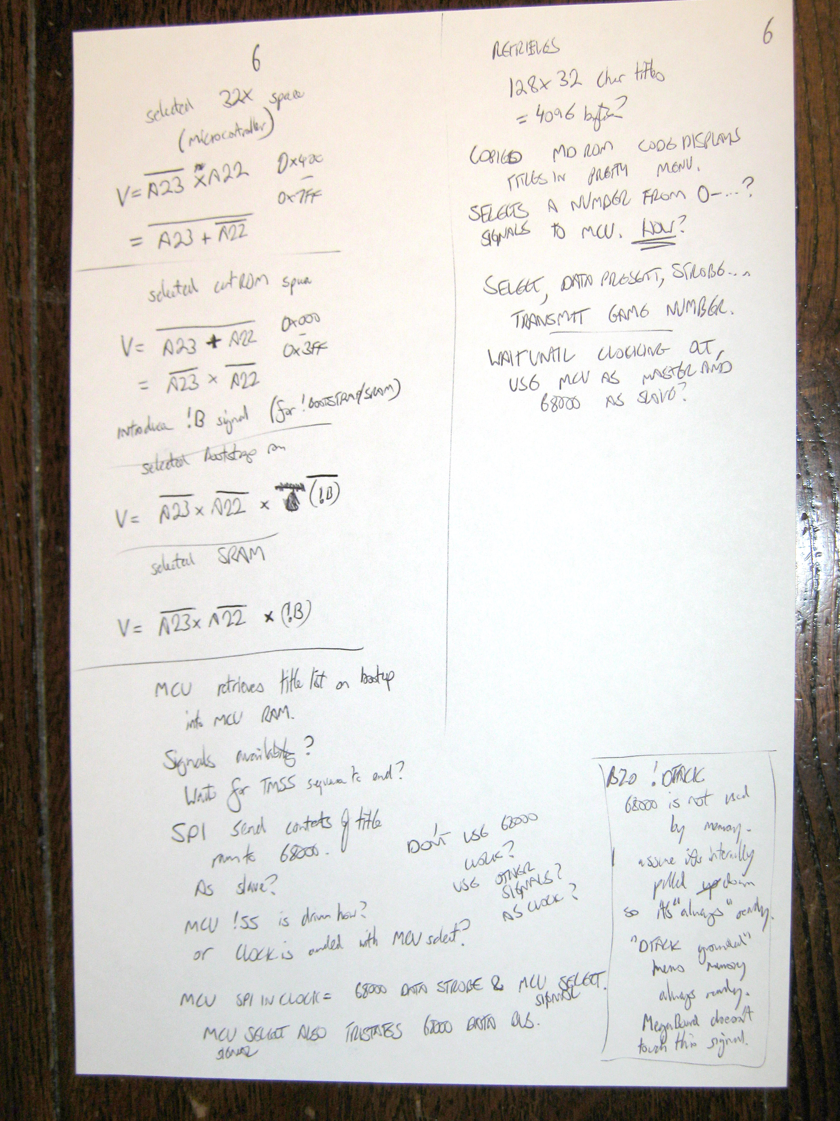
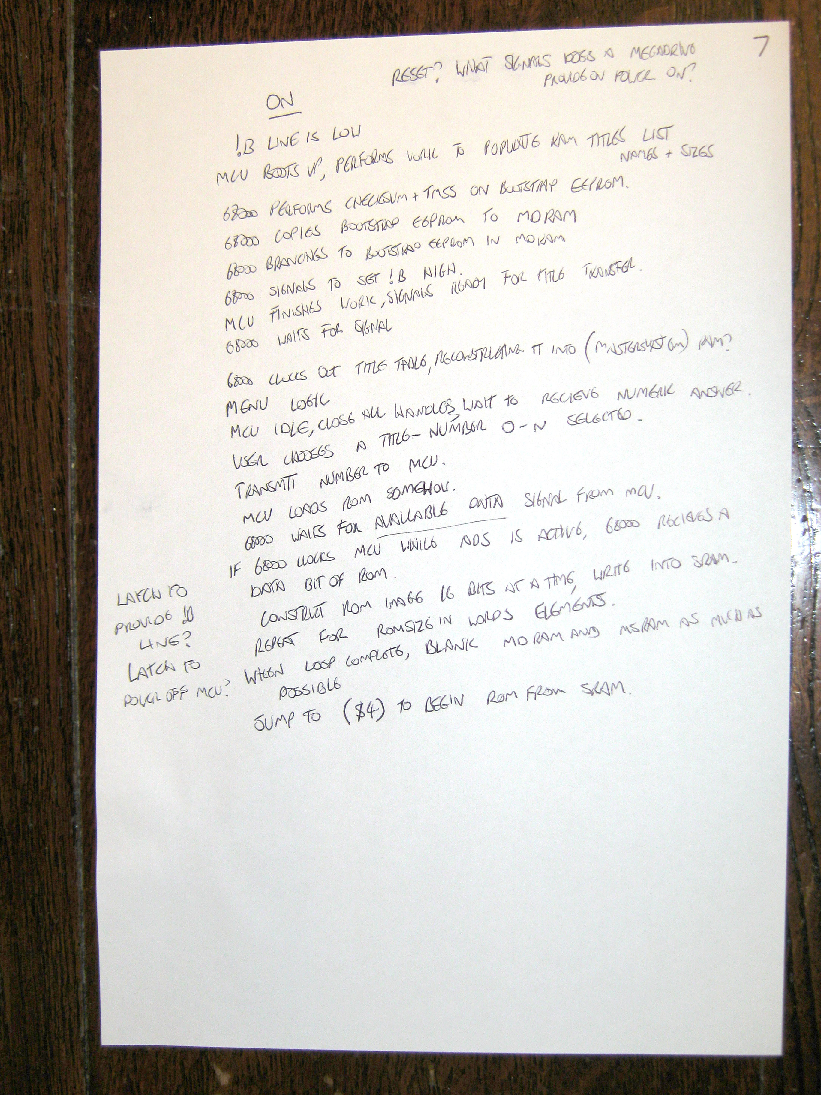
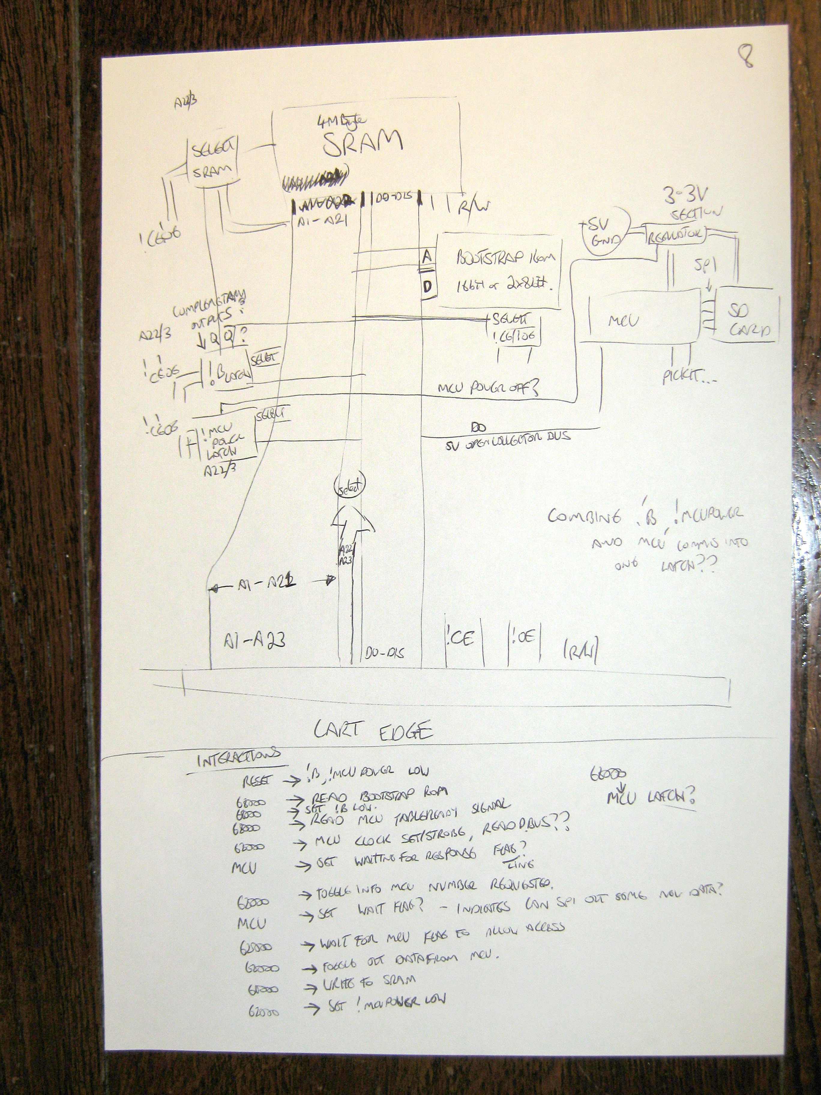
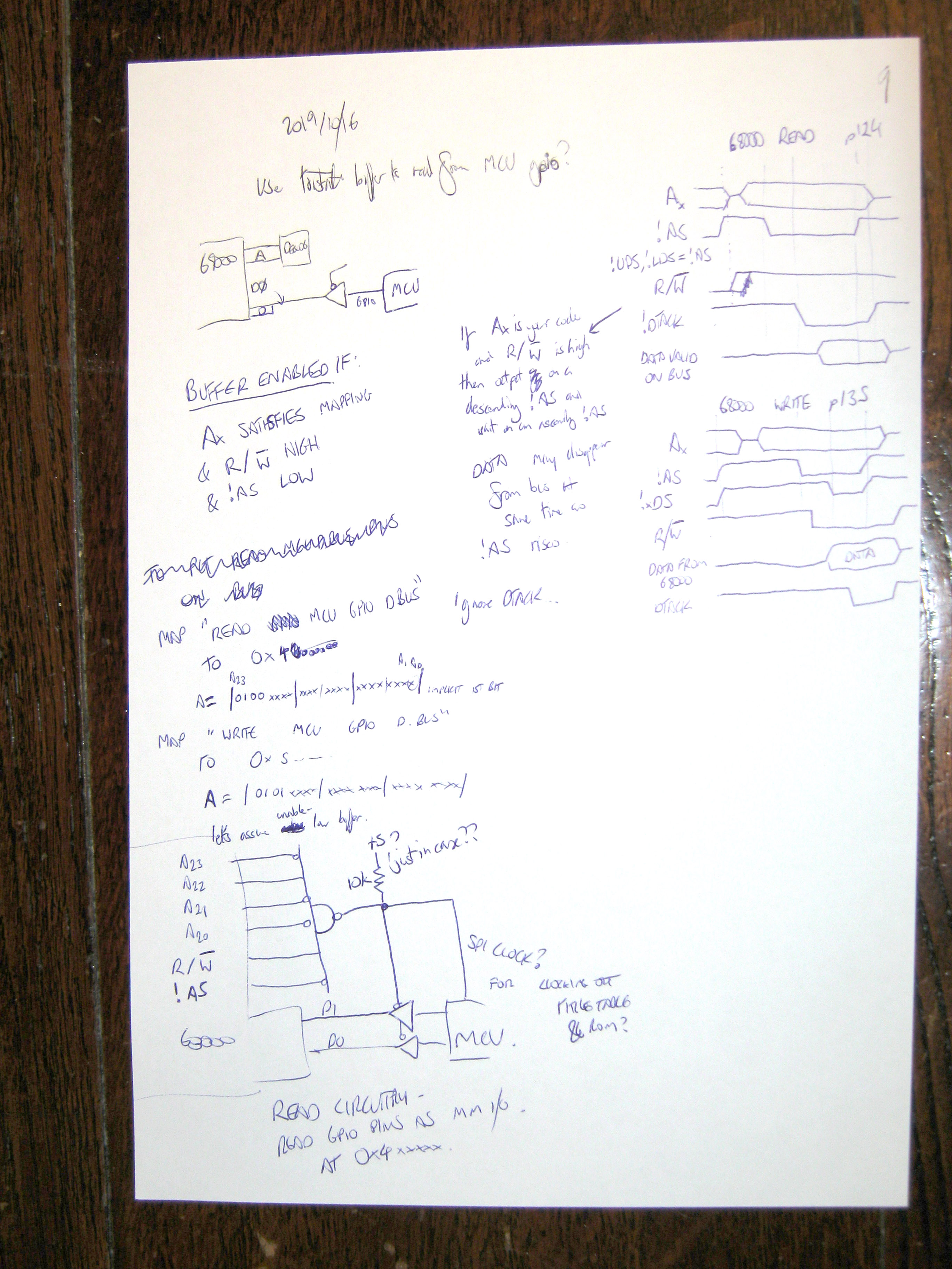
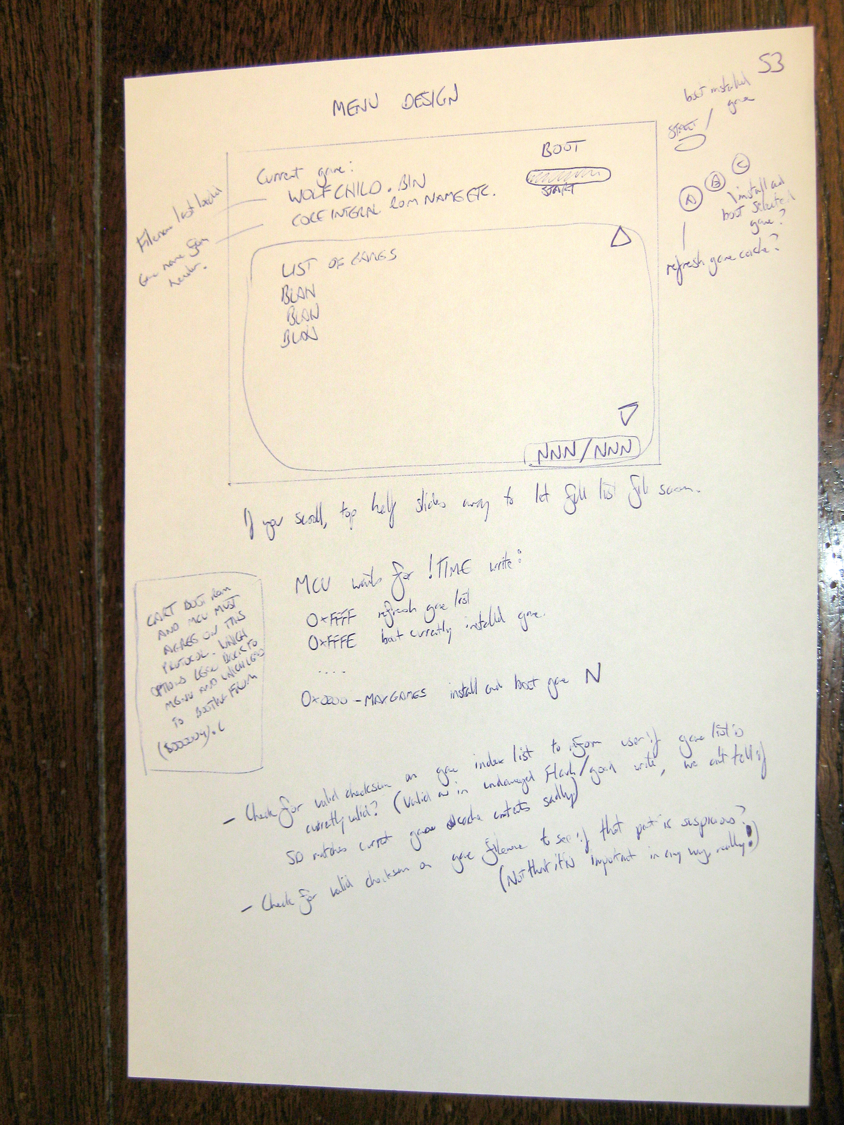
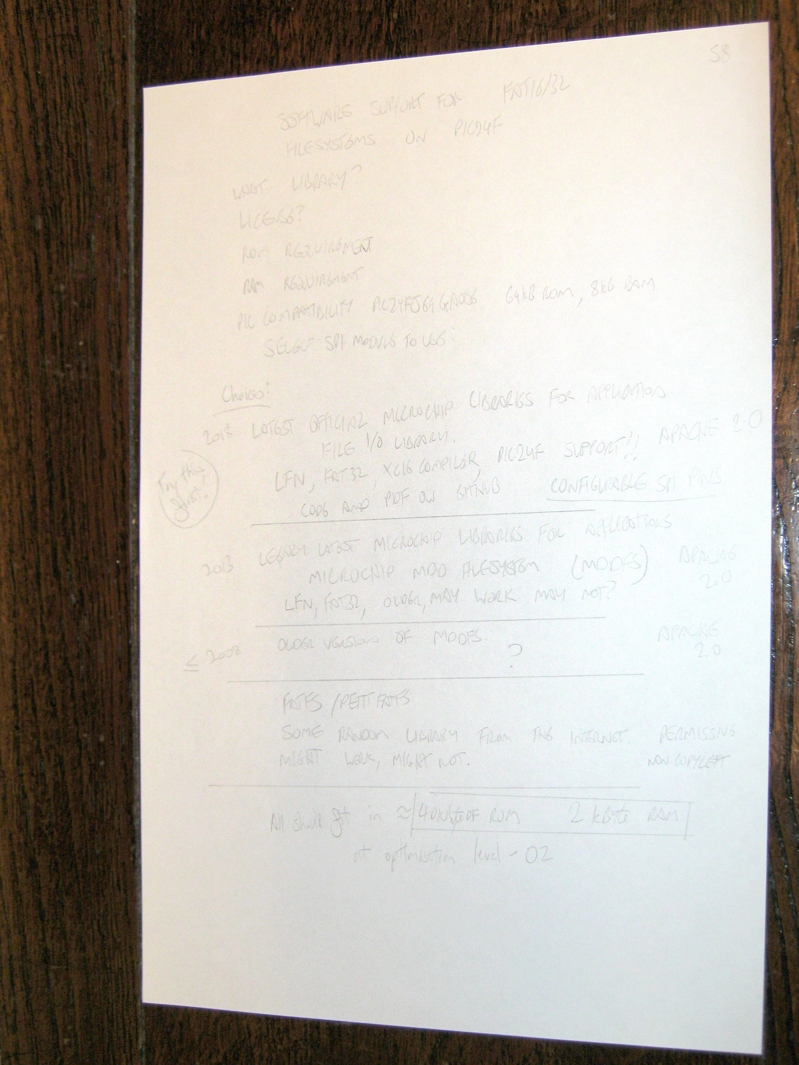
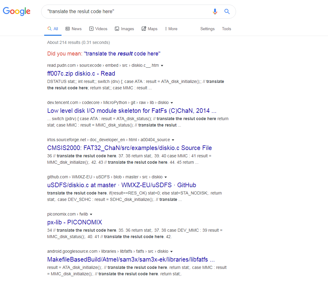
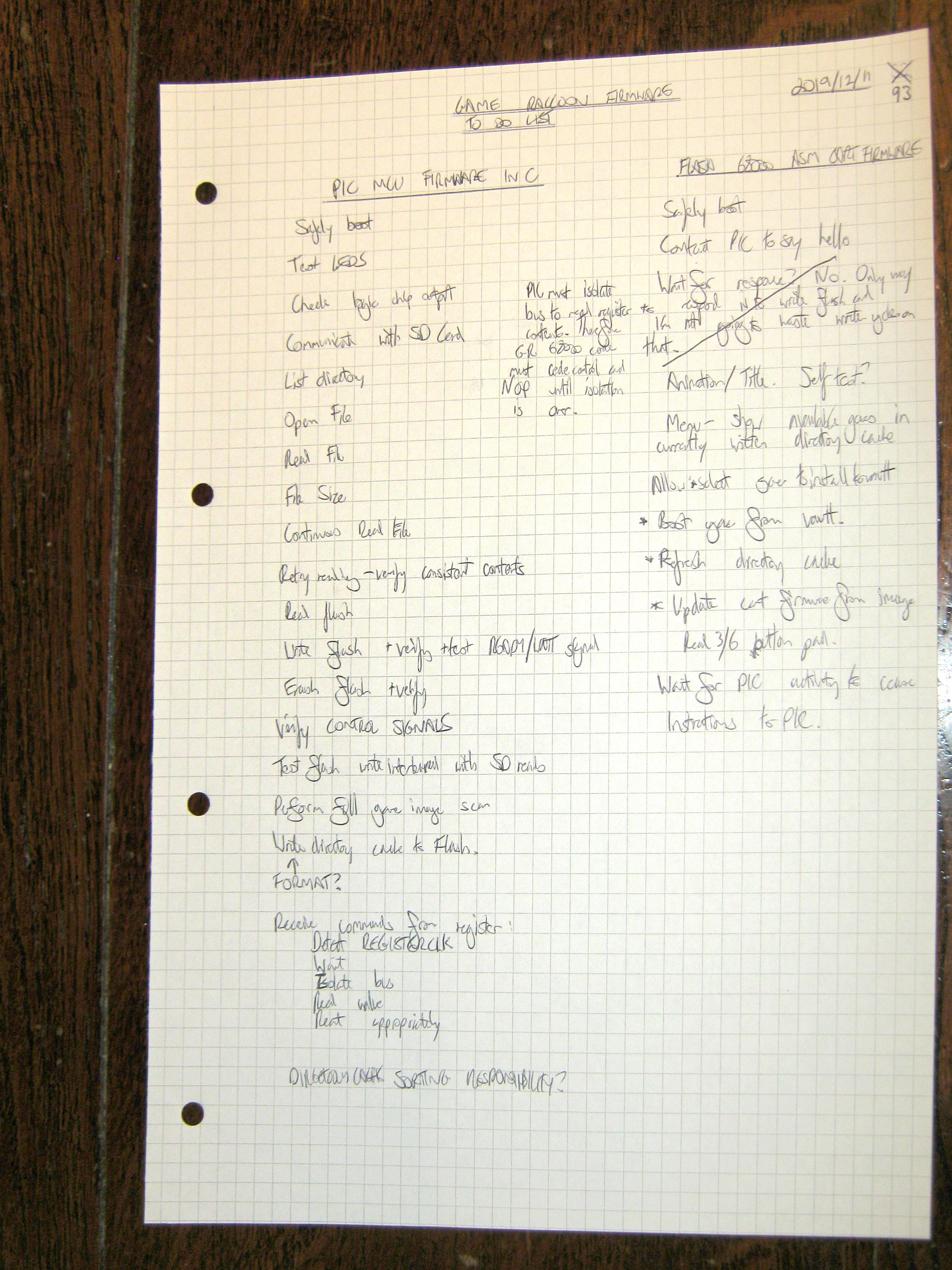
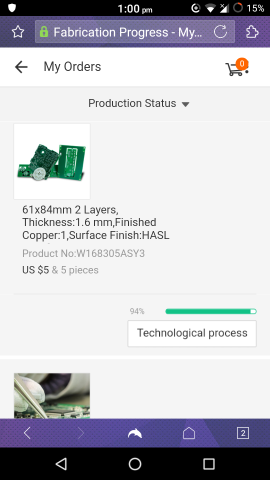
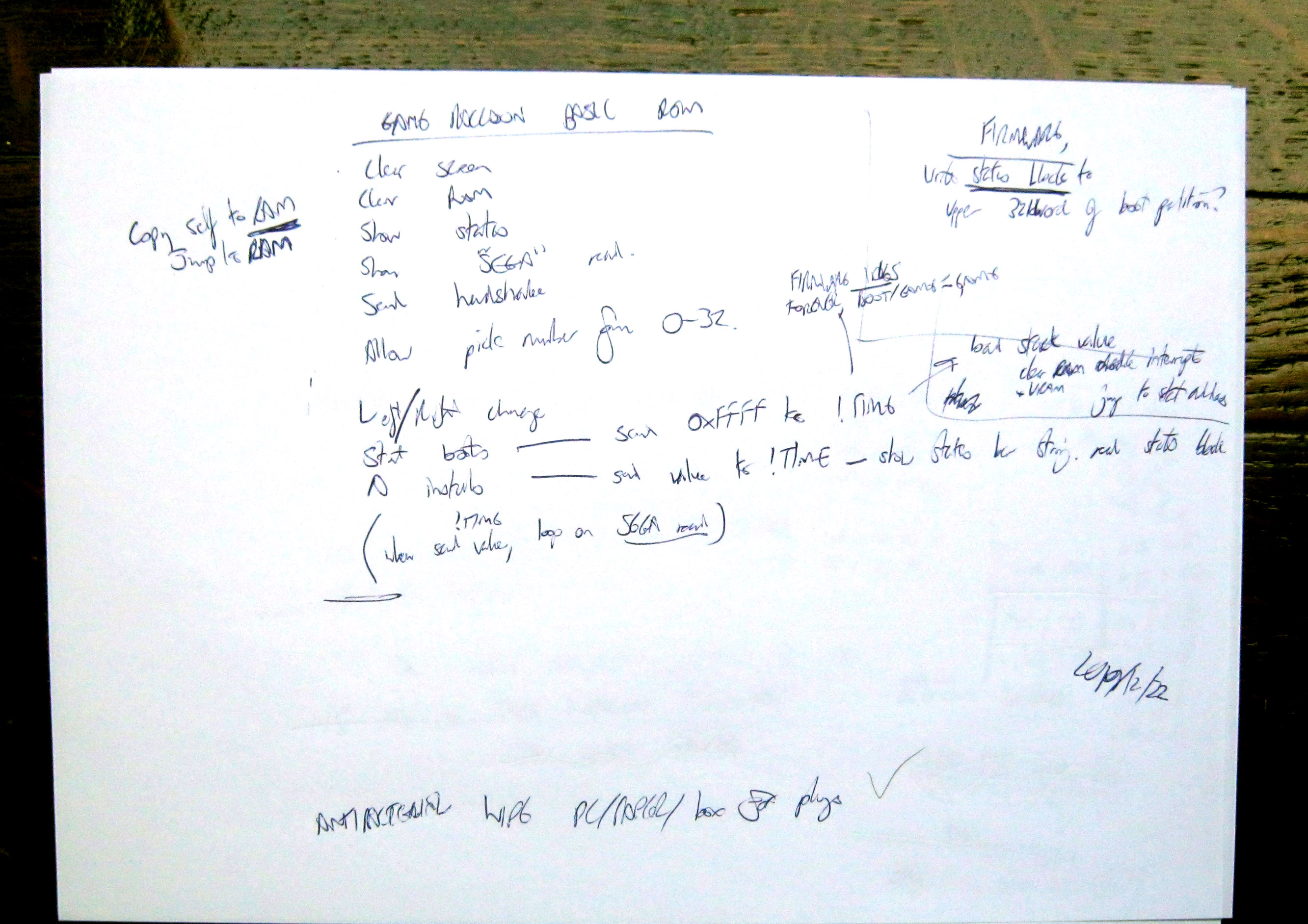
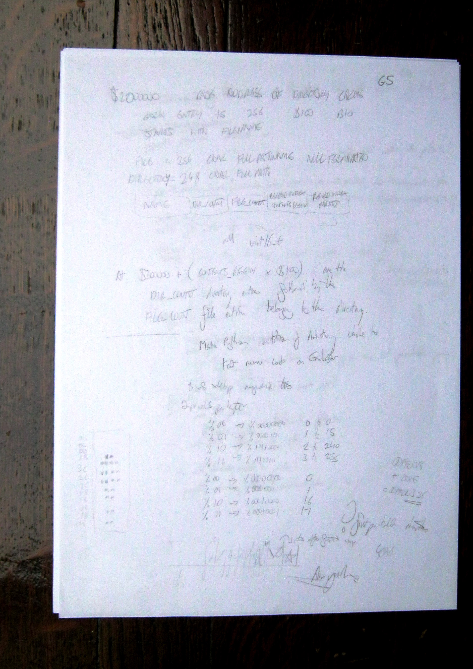
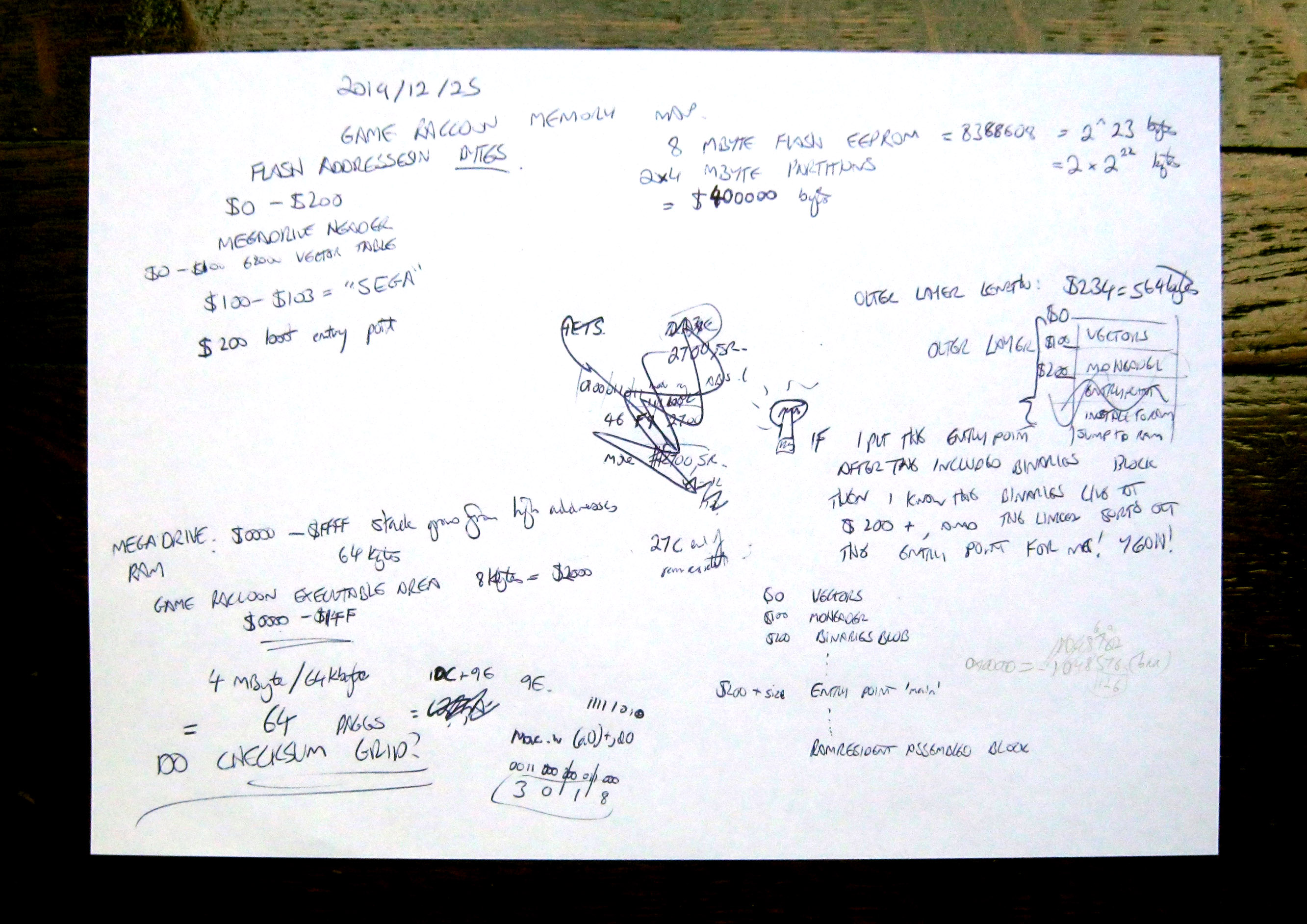
FatFs is really strange to me. Here's the description of it: "FatFs is a generic FAT/exFAT filesystem module for small embedded systems. The FatFs module is written in compliance with ANSI C (C89) and completely separated from the disk I/O layer. Therefore it is independent of the platform. It can be incorporated into small microcontrollers with limited resource, such as 8051, PIC, AVR, ARM, Z80, RX and etc. Also Petit FatFs module for tiny microcontrollers is available here." "Since FatFs module is the filesystem layer independent of platforms and storage media, it is completely separated from the physical devices, such as memory card, harddisk and any type of storage device. The low level device control module is not any part of FatFs module and it needs to be provided by implementer. FatFs accesses the storage devices via a simple media access interface shown below. Also sample implementations for some platforms are available in the downloads. A function checker for low level disk I/O module is available here." This means that it'll perform all the operations that the FAT filesystem requires, as long as you provide a way for it to read and write sectors to a physical device. Since that means diving into the SD card specification somewhat, I was kinda hoping that that would be something the library would do for me. I'm incredibly lucky that in the sample implementations shipped with FatFs, there's a sample for PIC24! It's going to be set up for whatever application the person who used it last wanted it for, but I ought to be able to untangle it. Let's have a look. Okay. The 
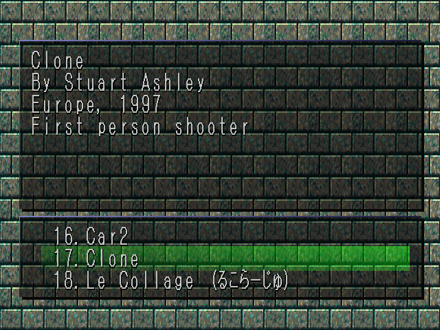
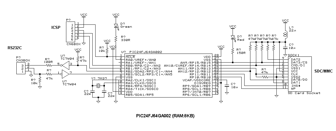
ffsample\pic24 directory contains instructions for building a breadboard project based on the PIC24FJ64GA002, a DIP PIC similar to the one used in the PSCD32. It's a complicated beast, but I think I can tilt my head and intuit what it's intended to be. It has the standard power connections, connects to a PICKIT, connects to an SD card through SPI, but the user interface is a serial terminal. In the sample program, the user can use a PC with a serial connection to send text commands to the project, and it'll output data and status updates back to you. I need to unravel what parts of this are important and what aren't. Ideally, I'd like to find a set of functions which provide the necessary missing ham slice that FatFs needs to talk to an SD card, and I can leave the rest. 
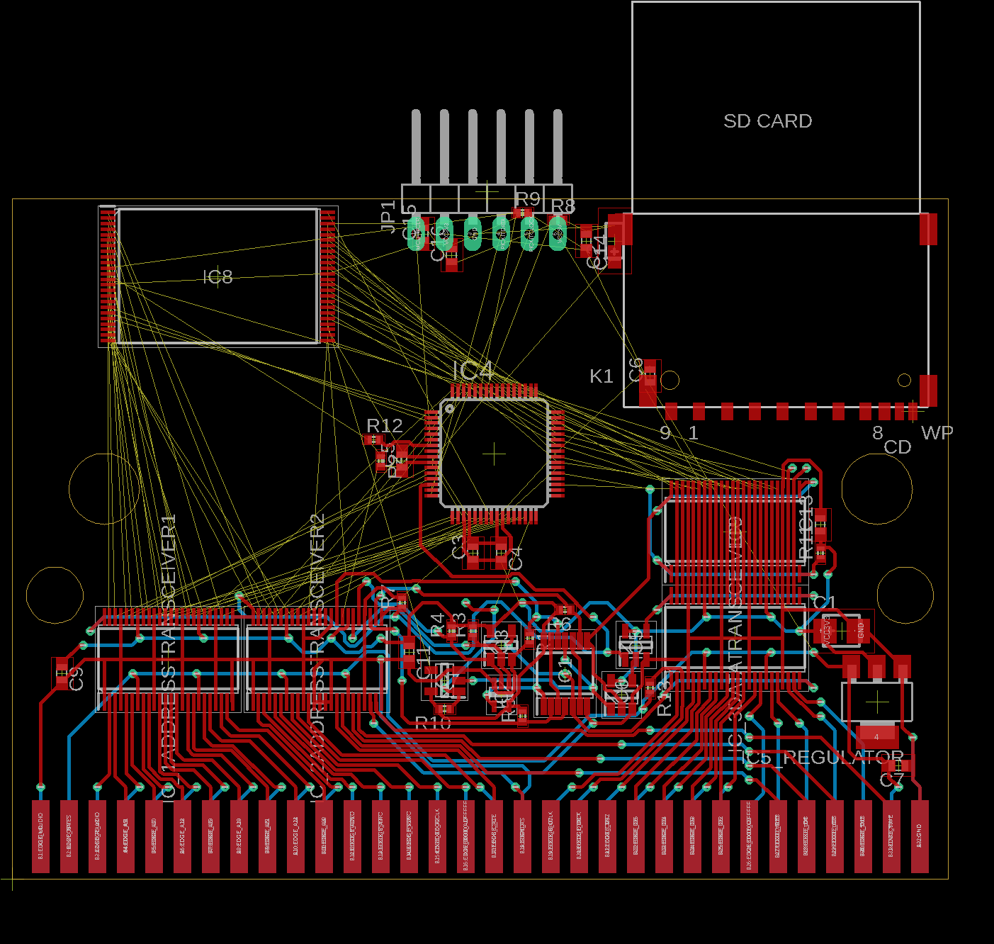
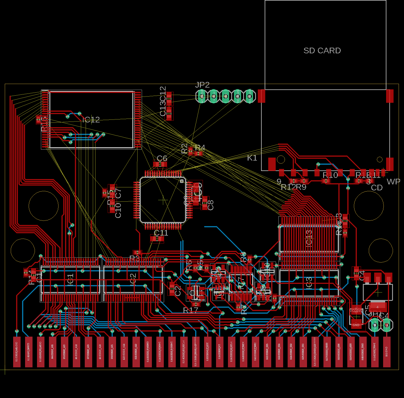
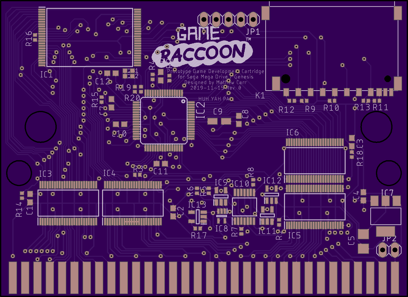
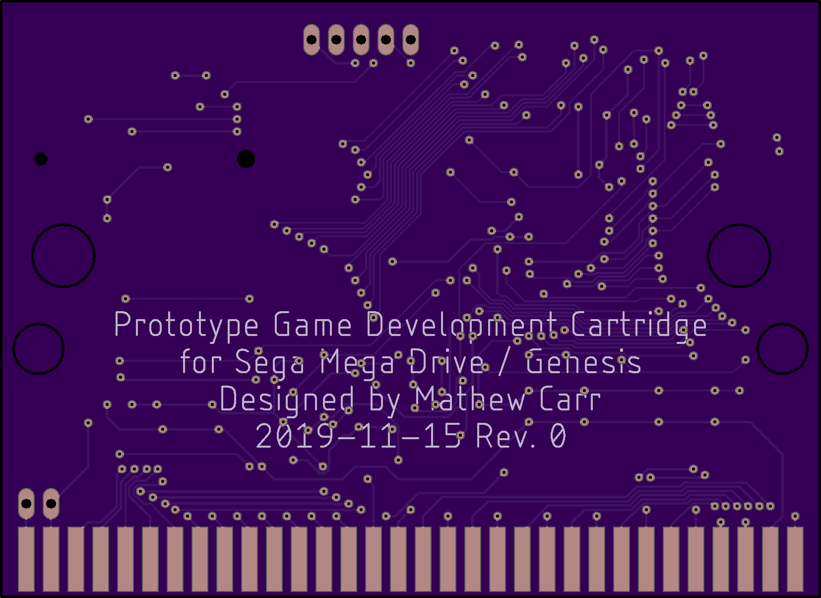
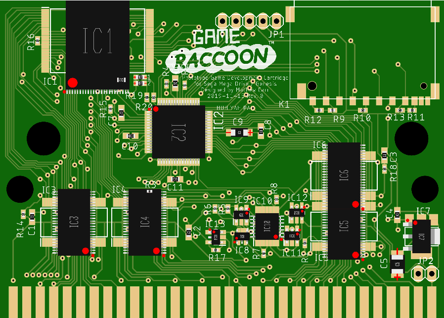
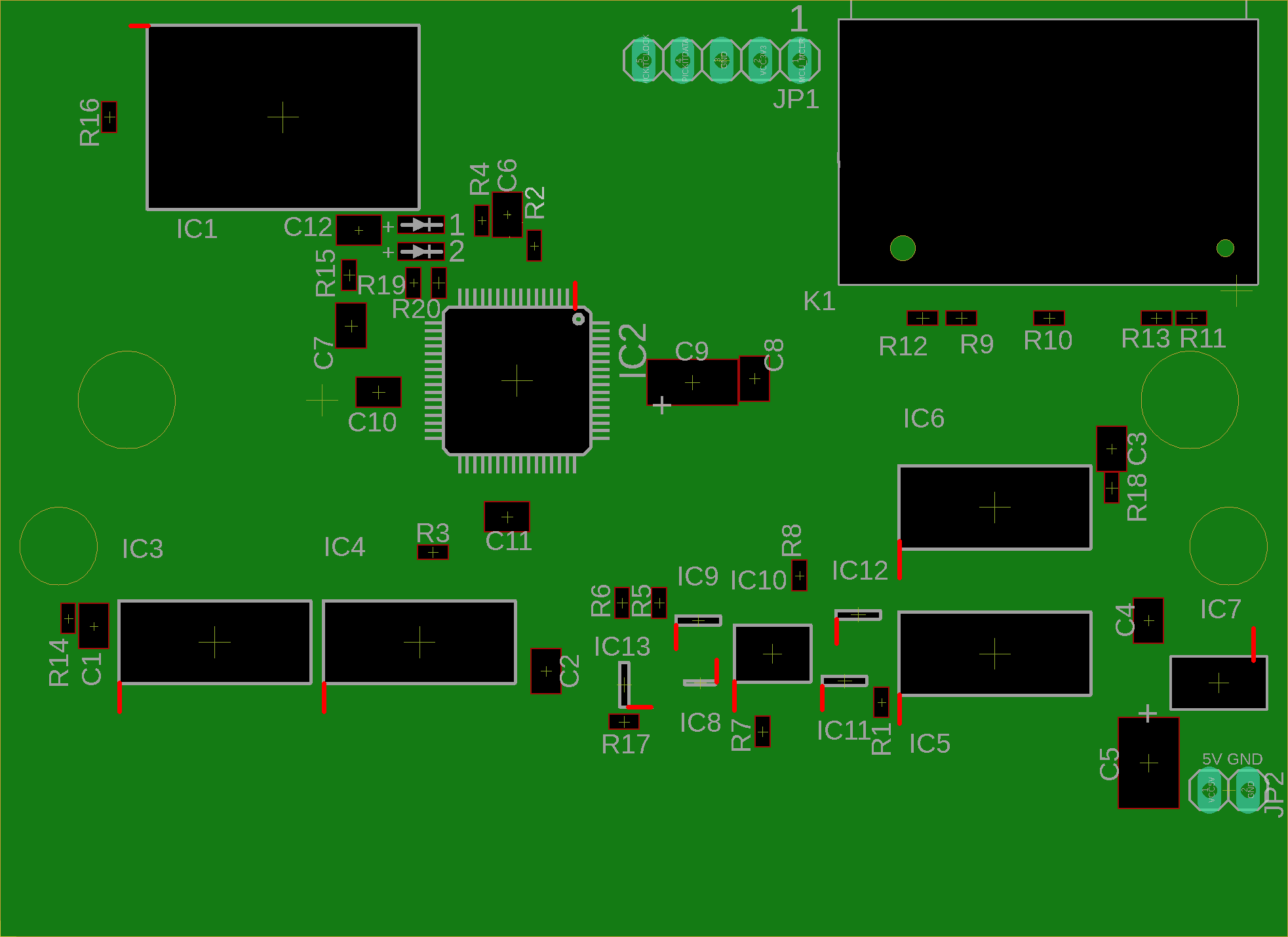
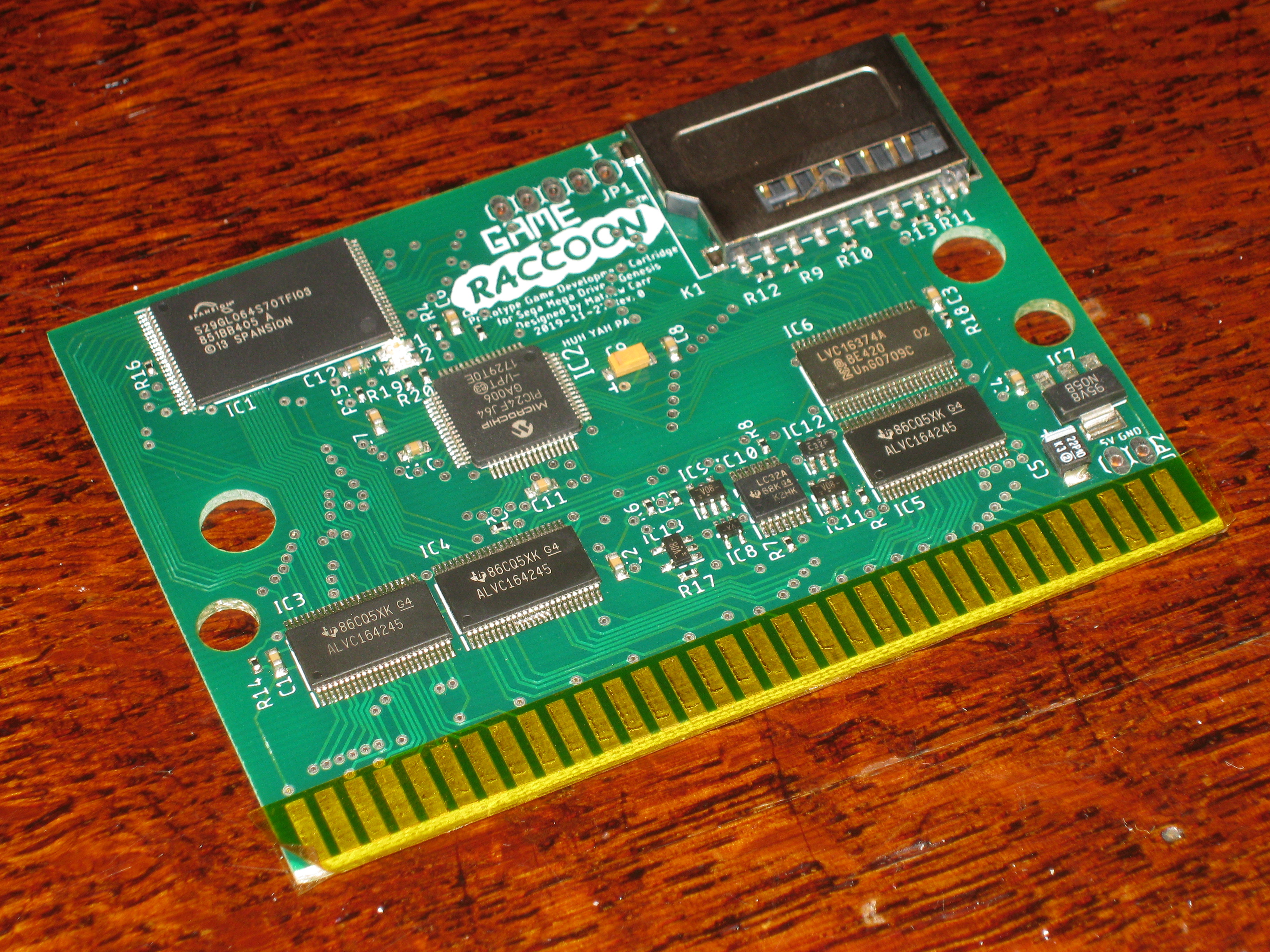
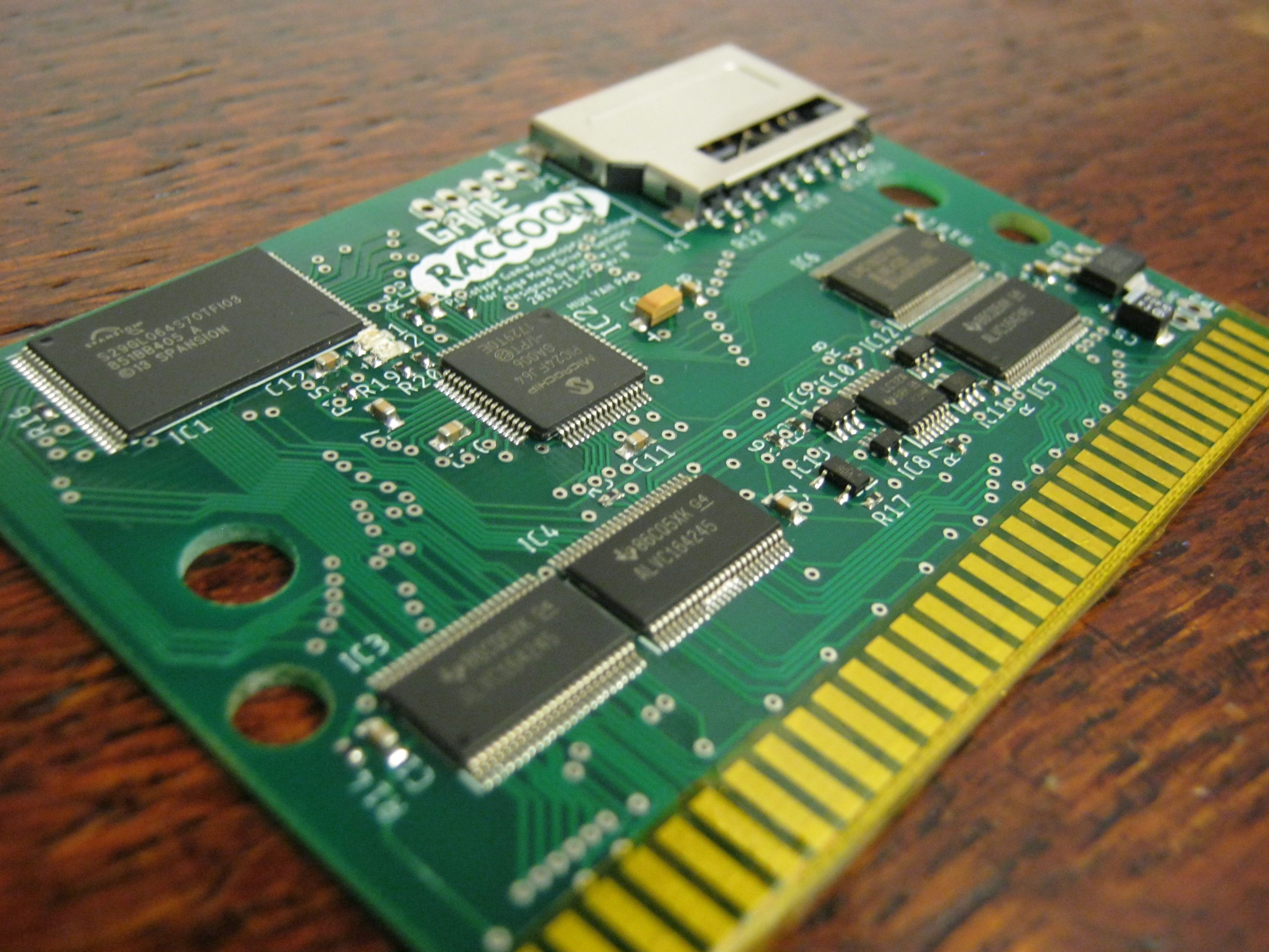
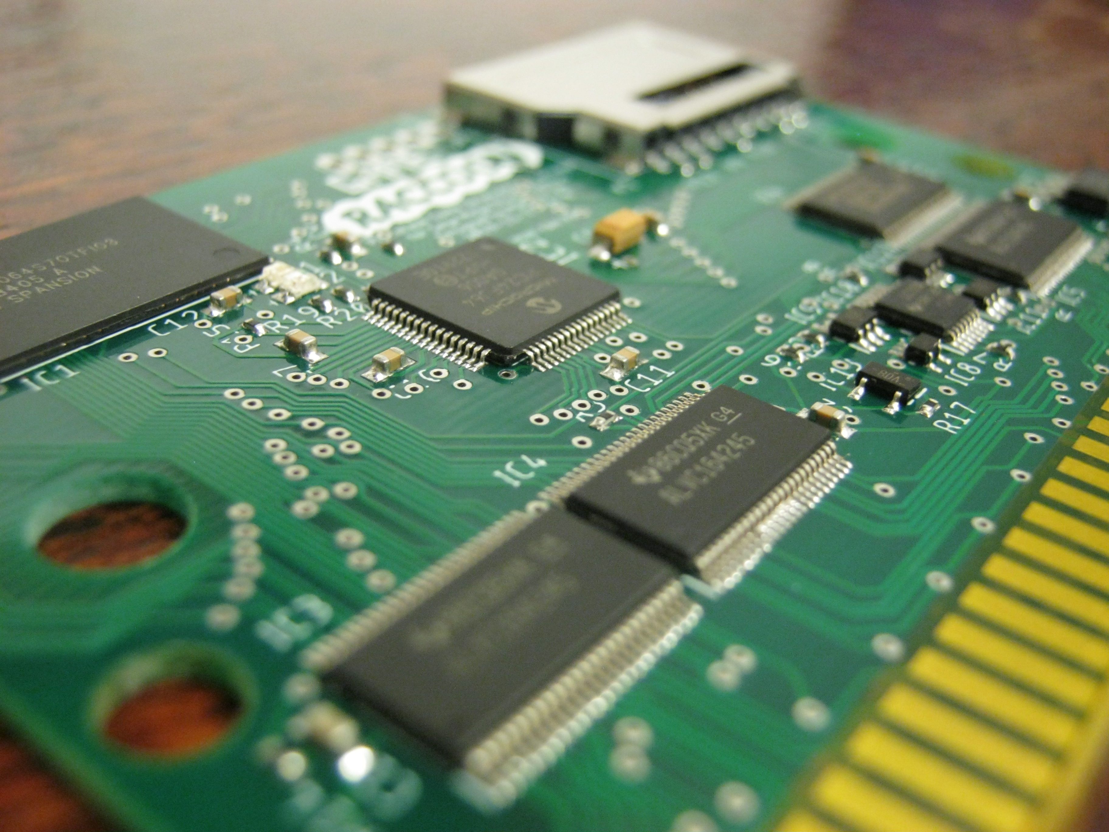
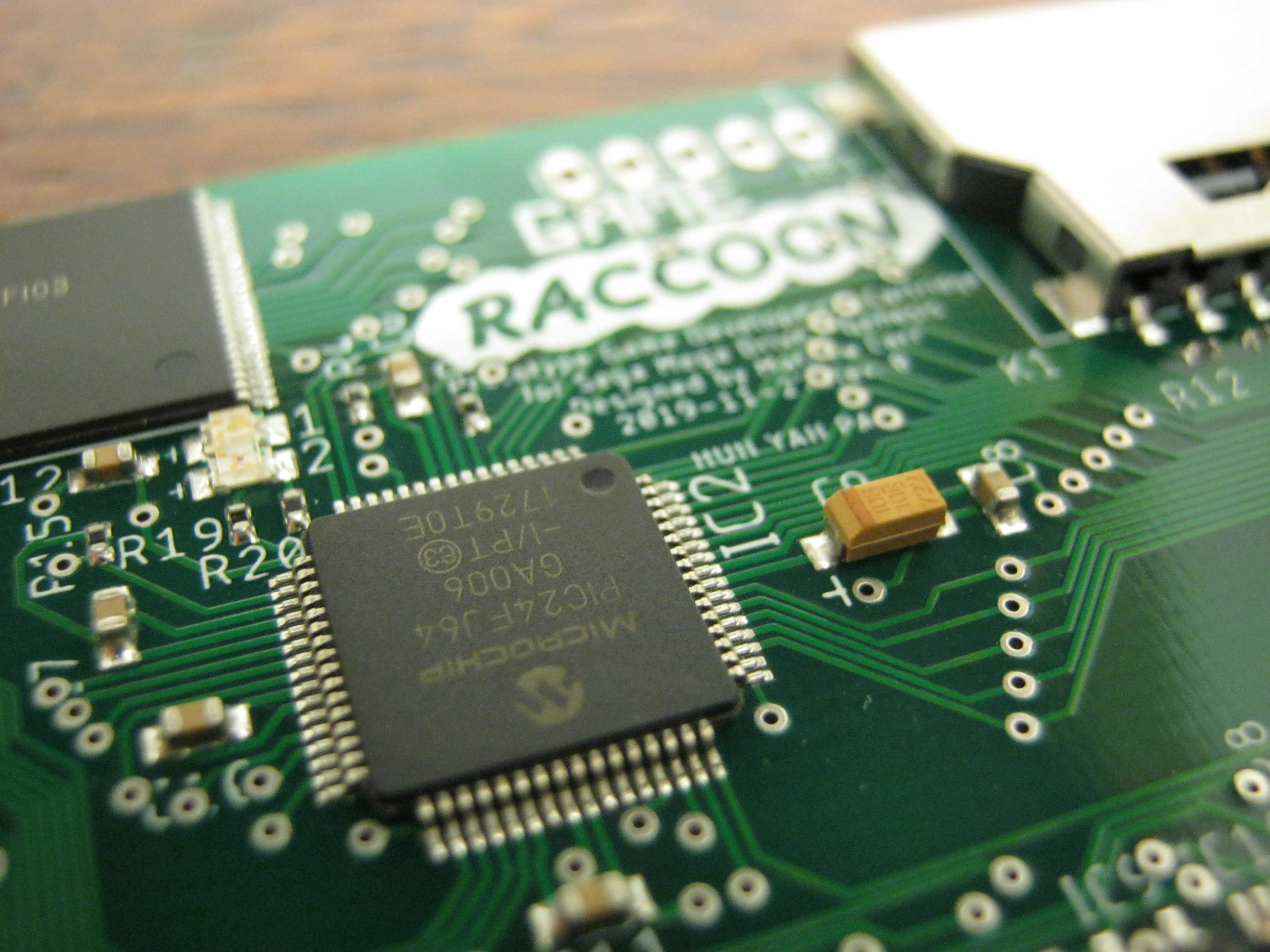
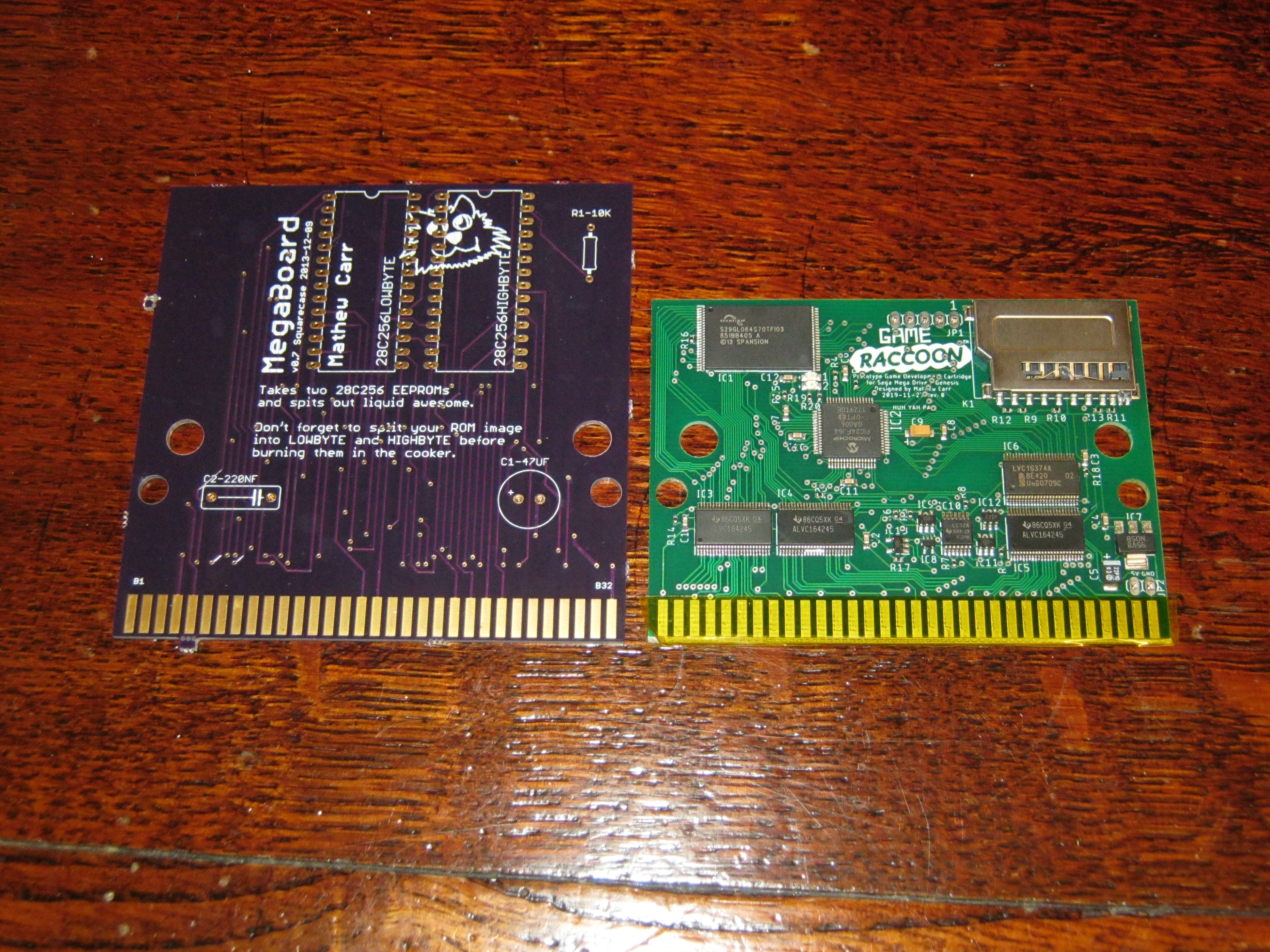
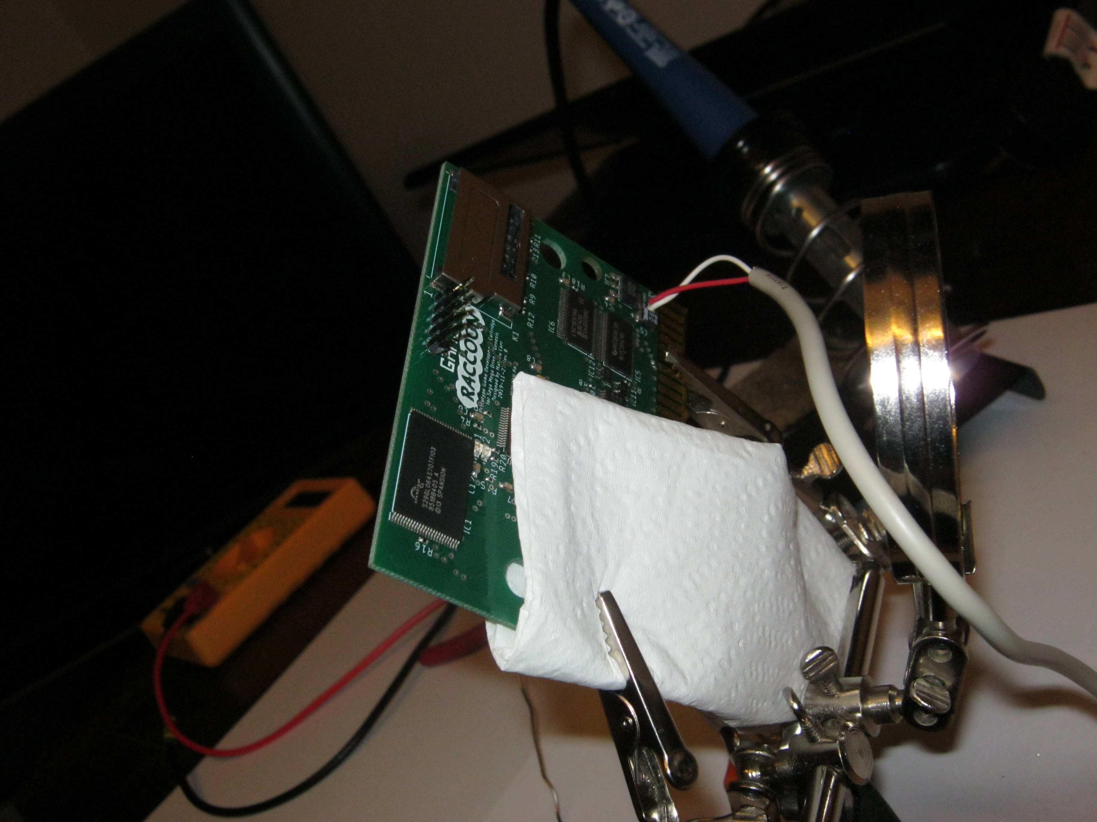
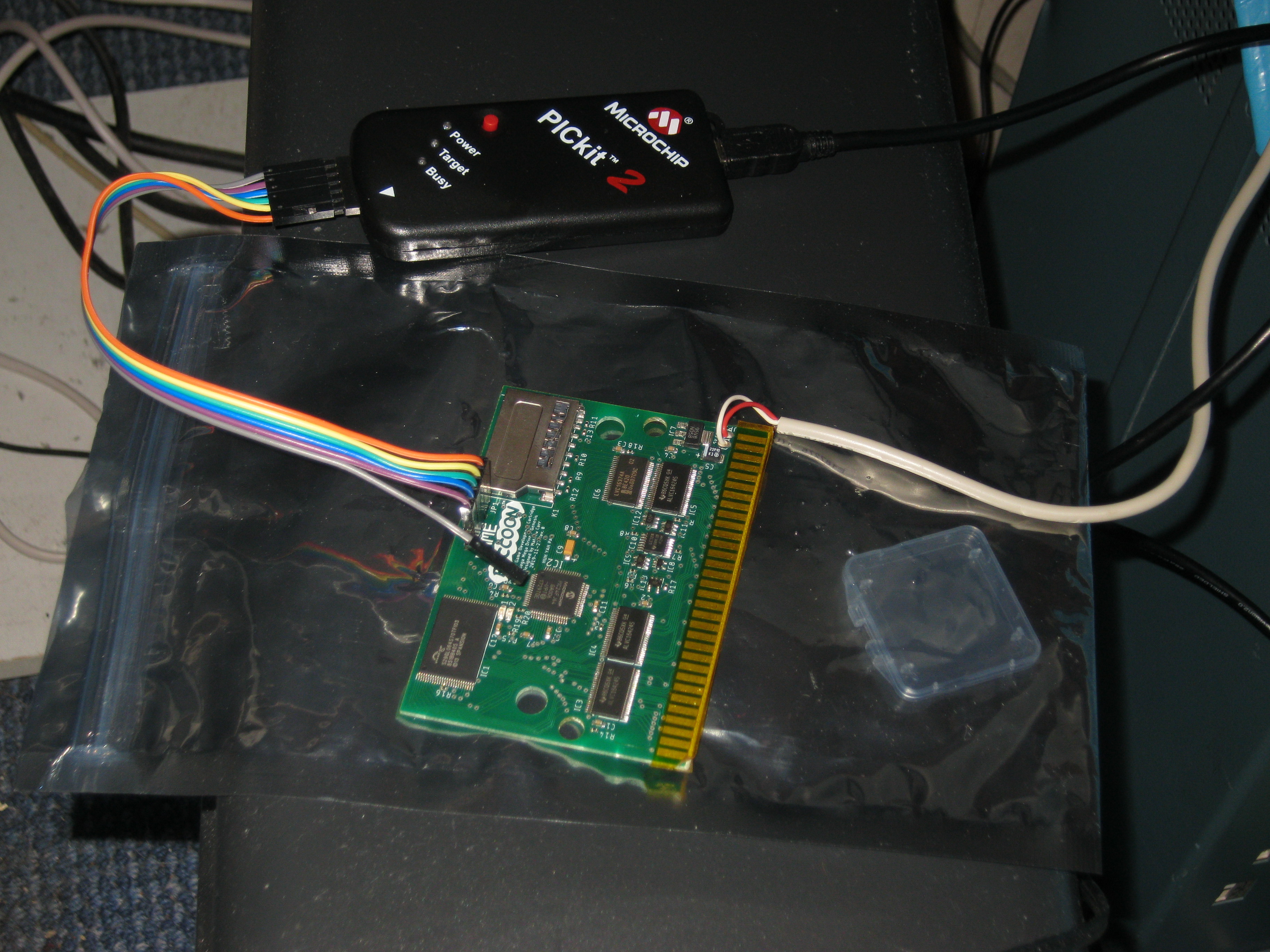
Surprisingly, it didn't take all that much adaptation to make this sample project work with the Game Raccoon board. 
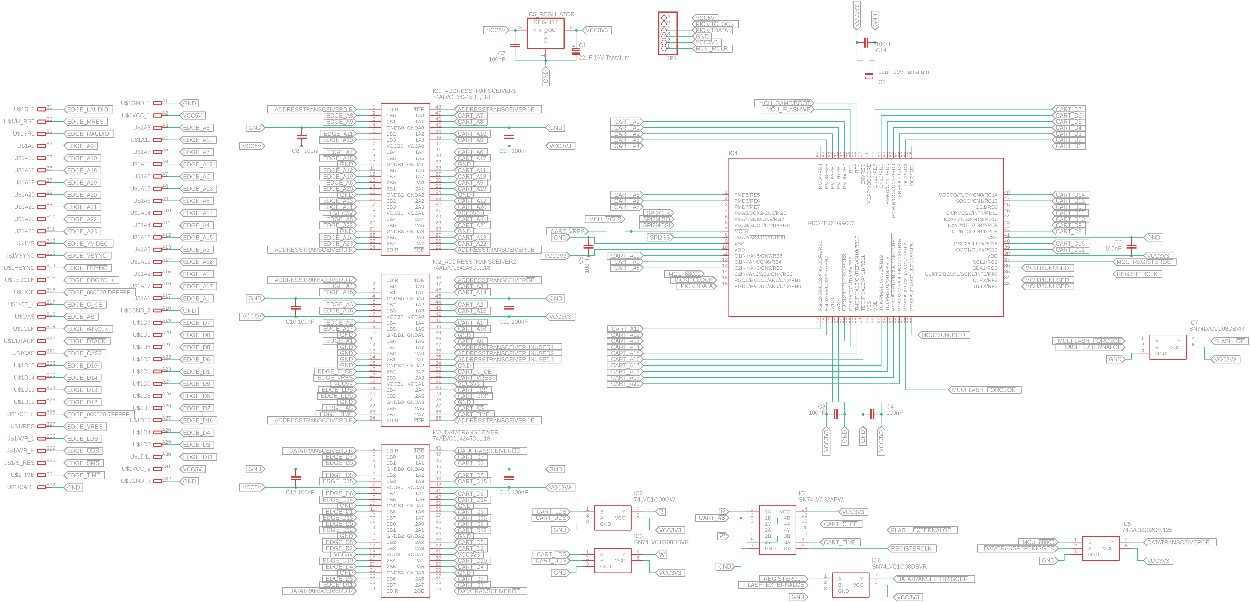
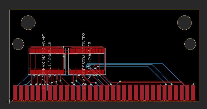
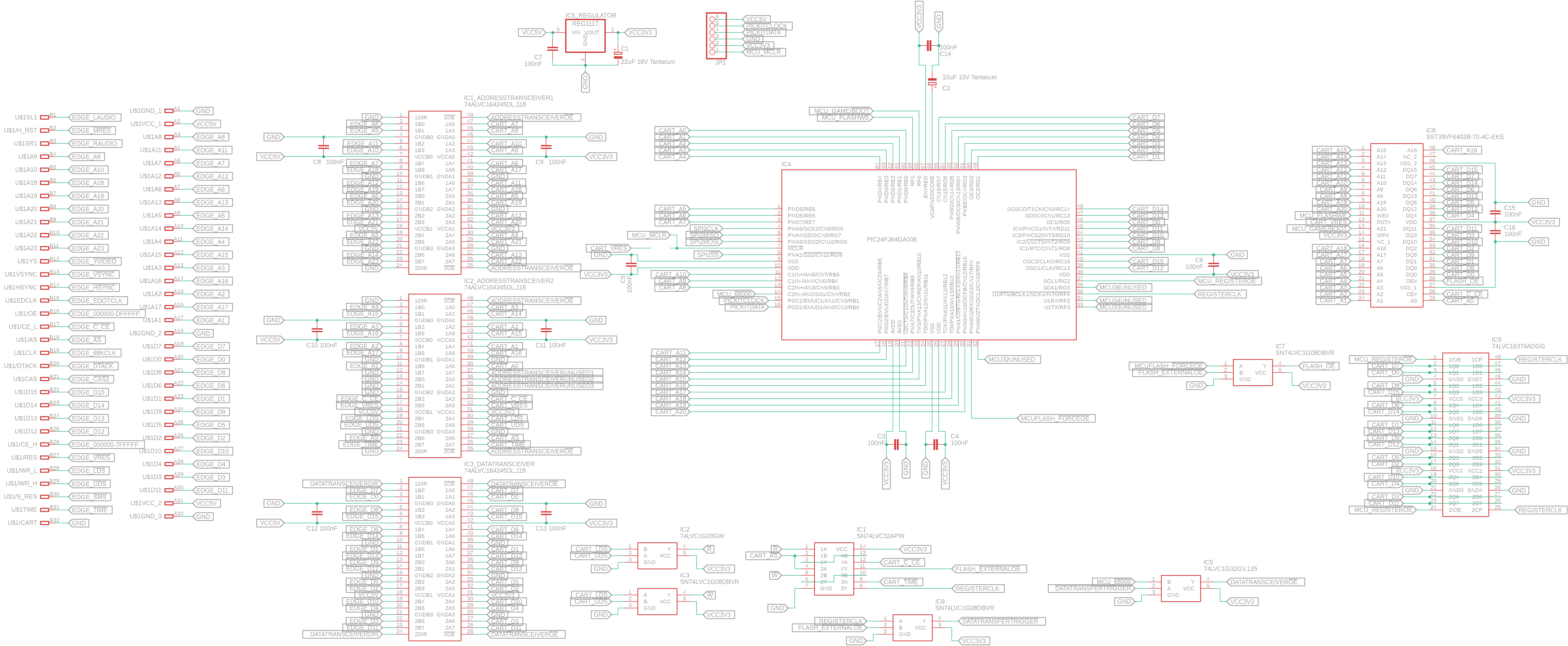
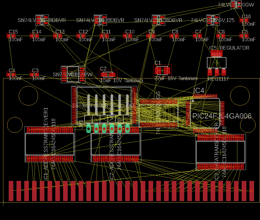
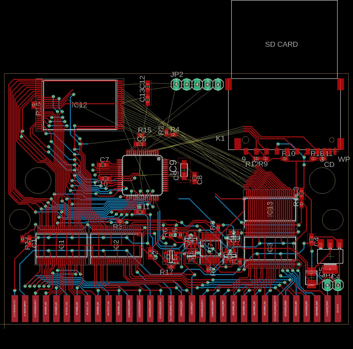
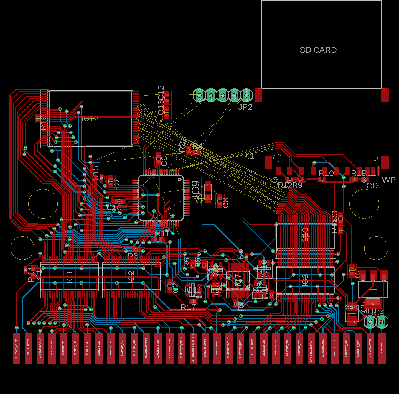
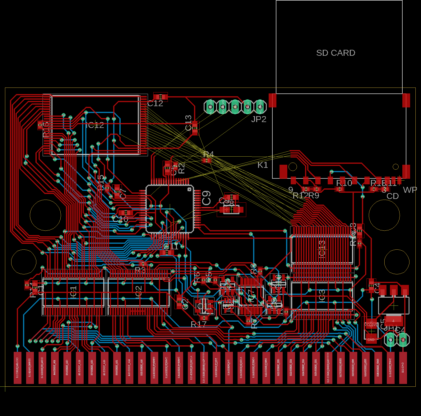
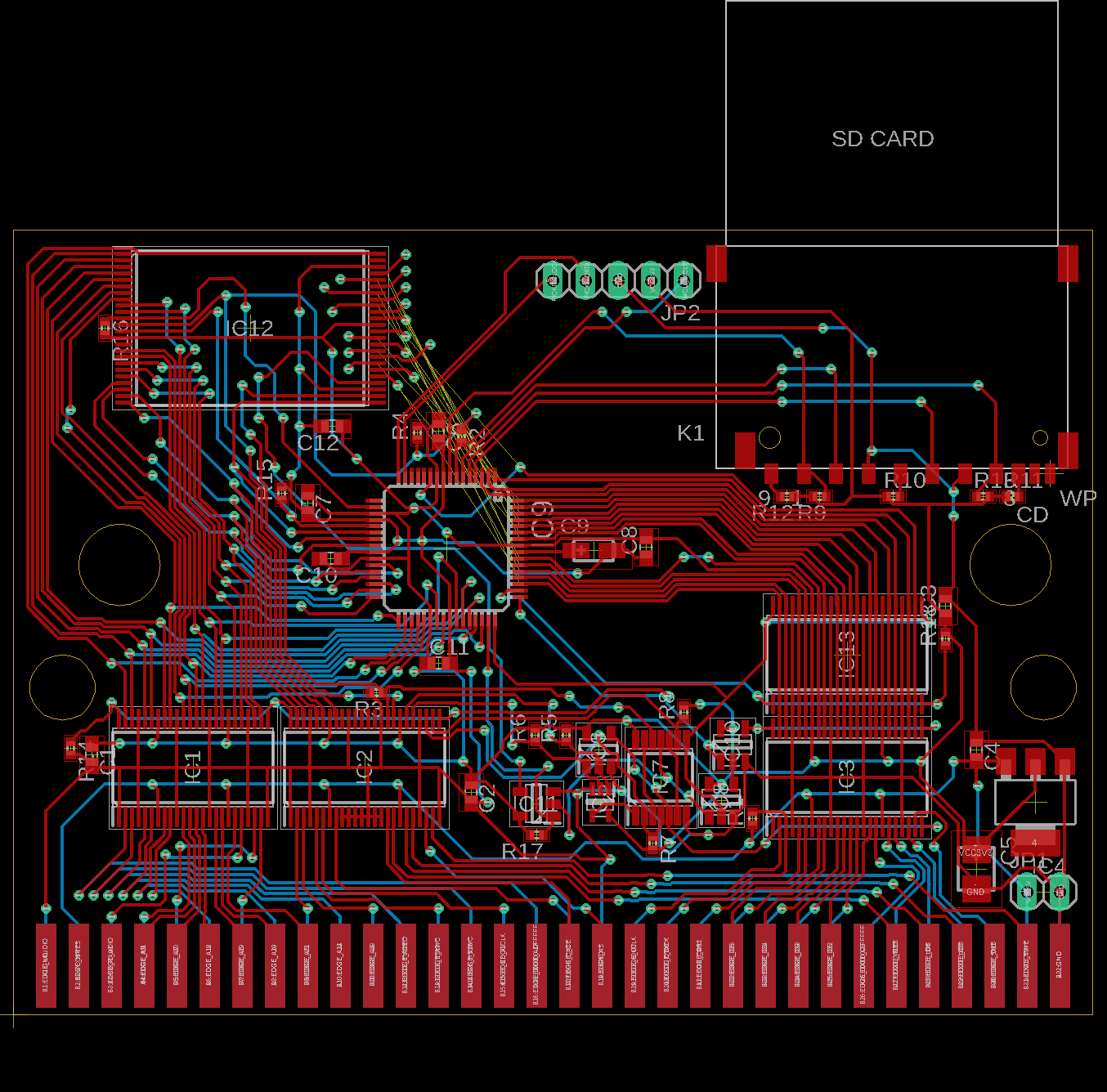
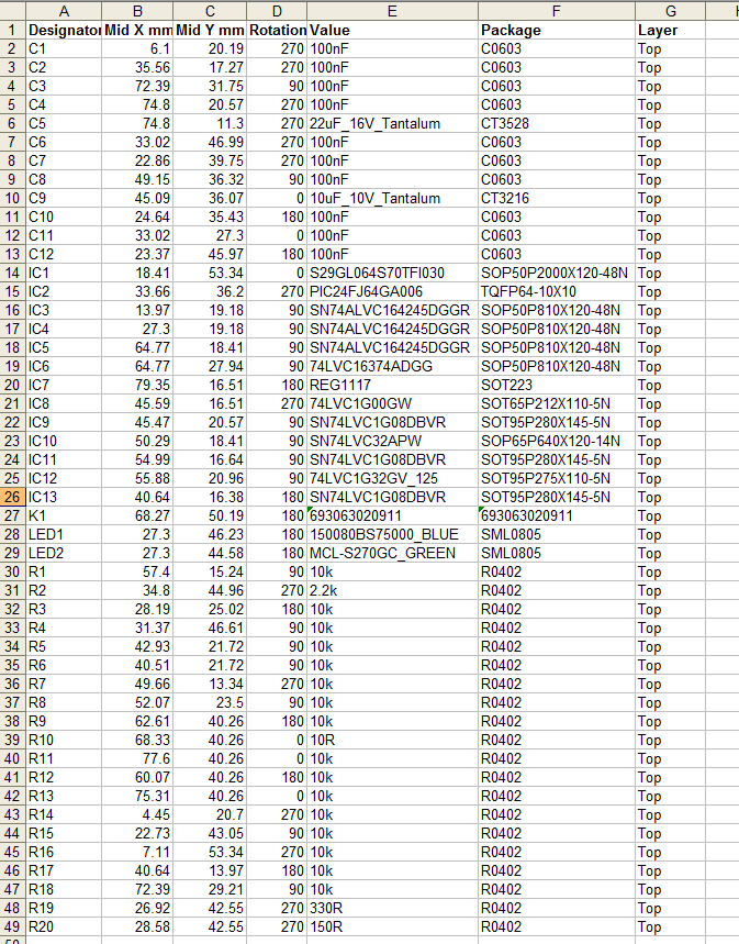
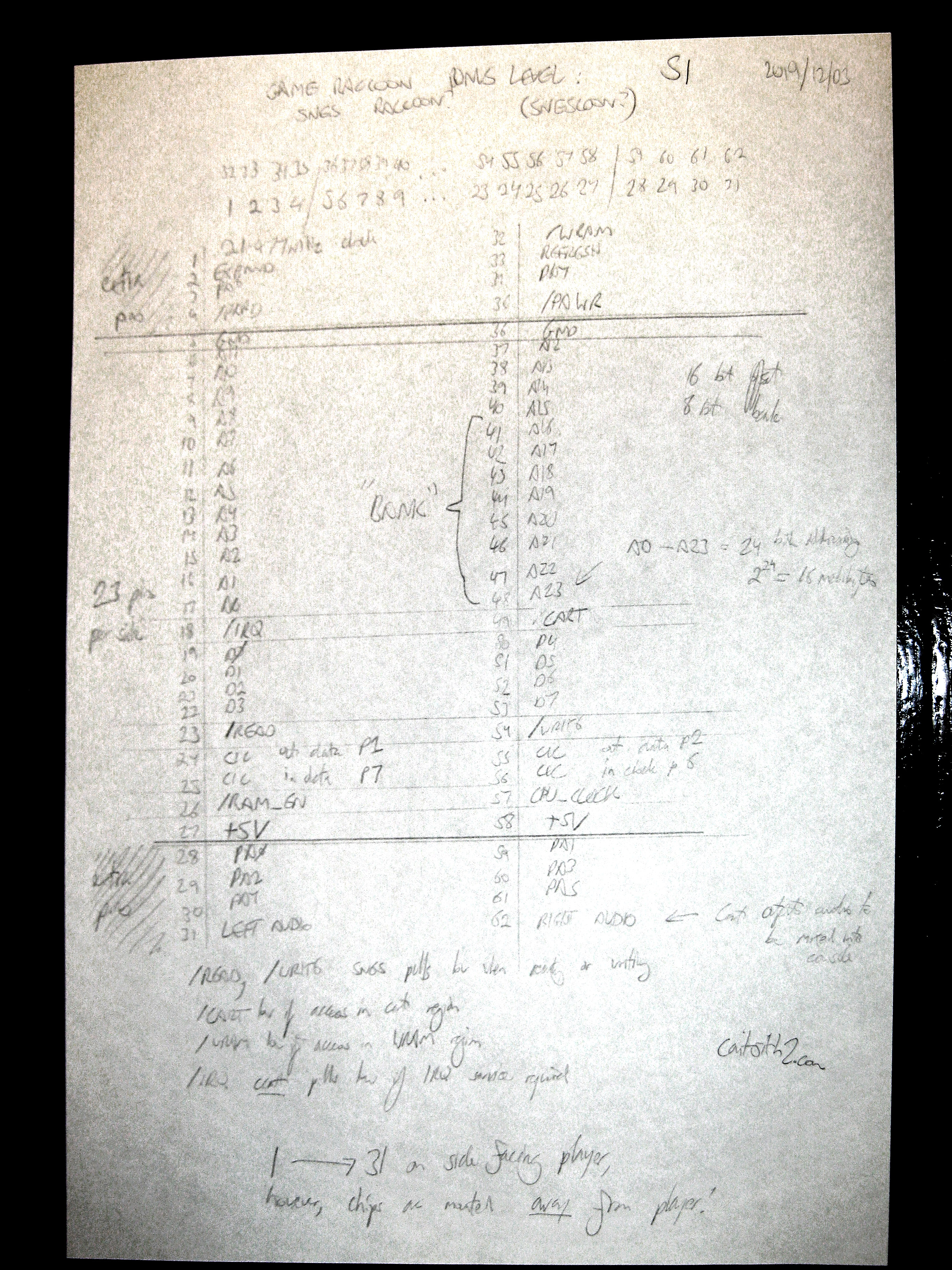
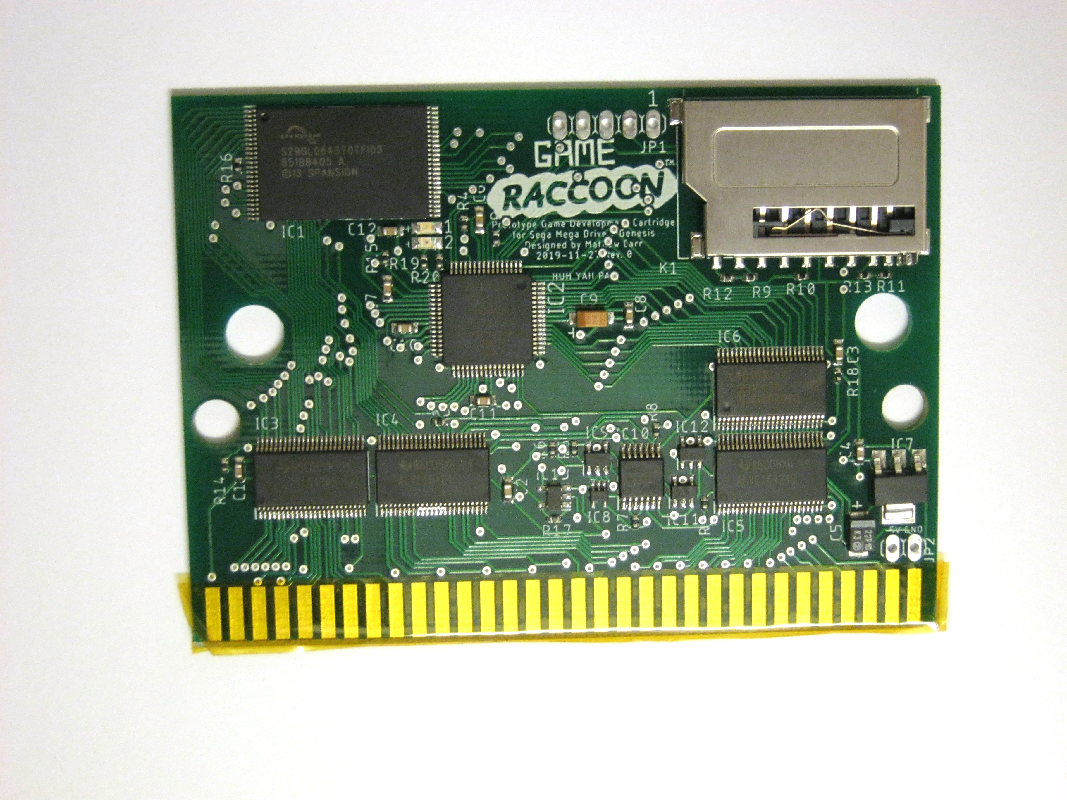
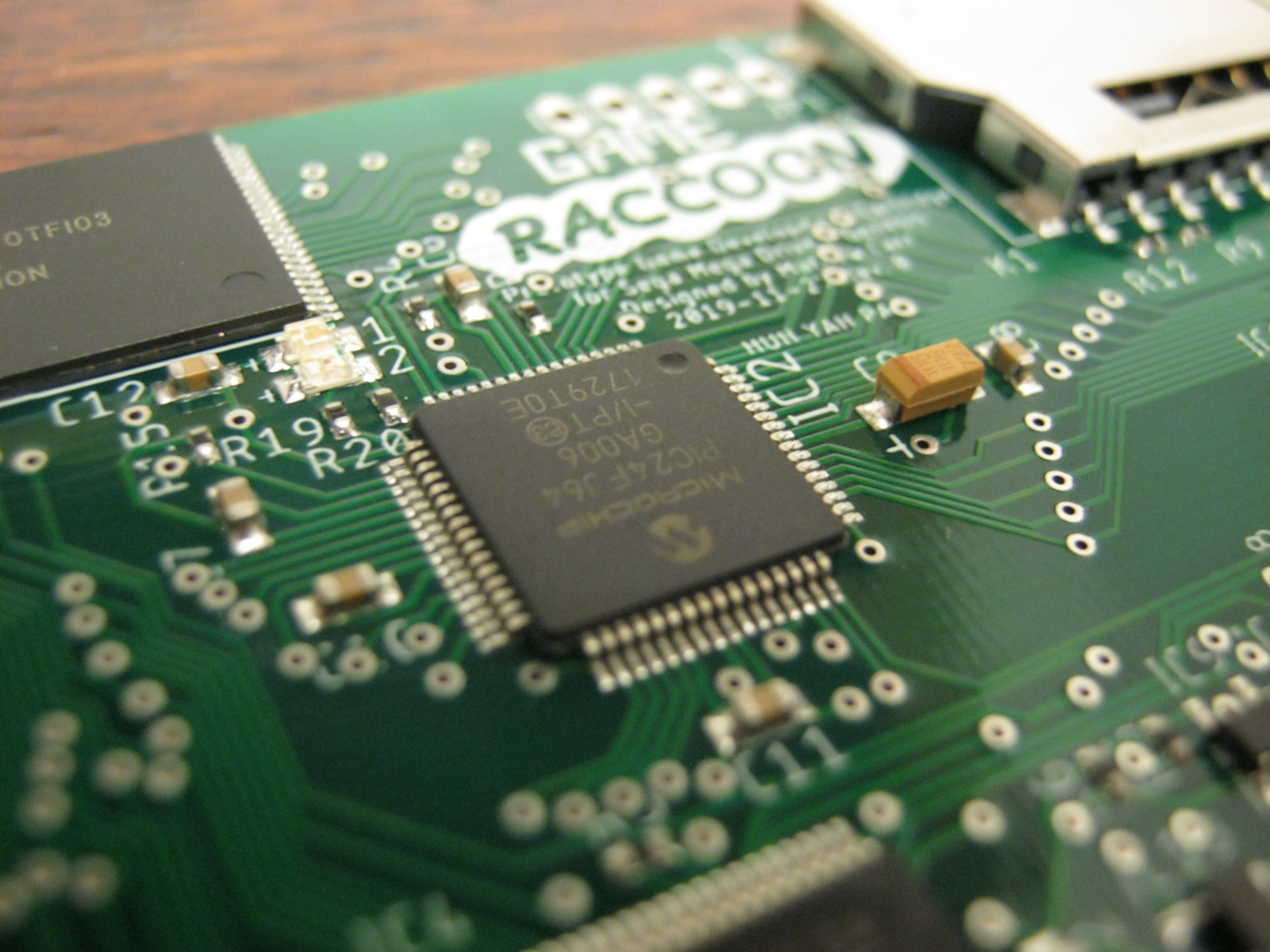
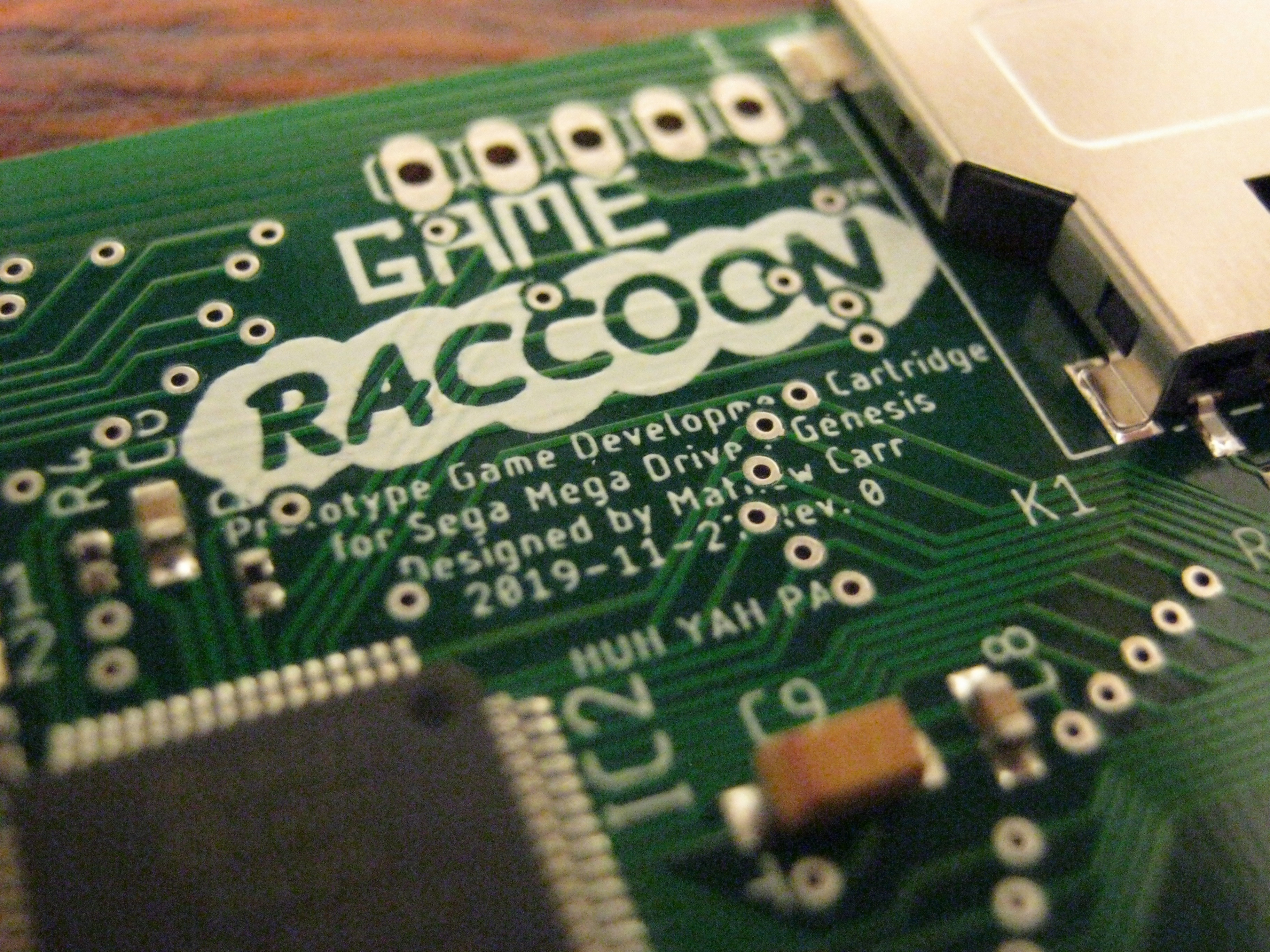
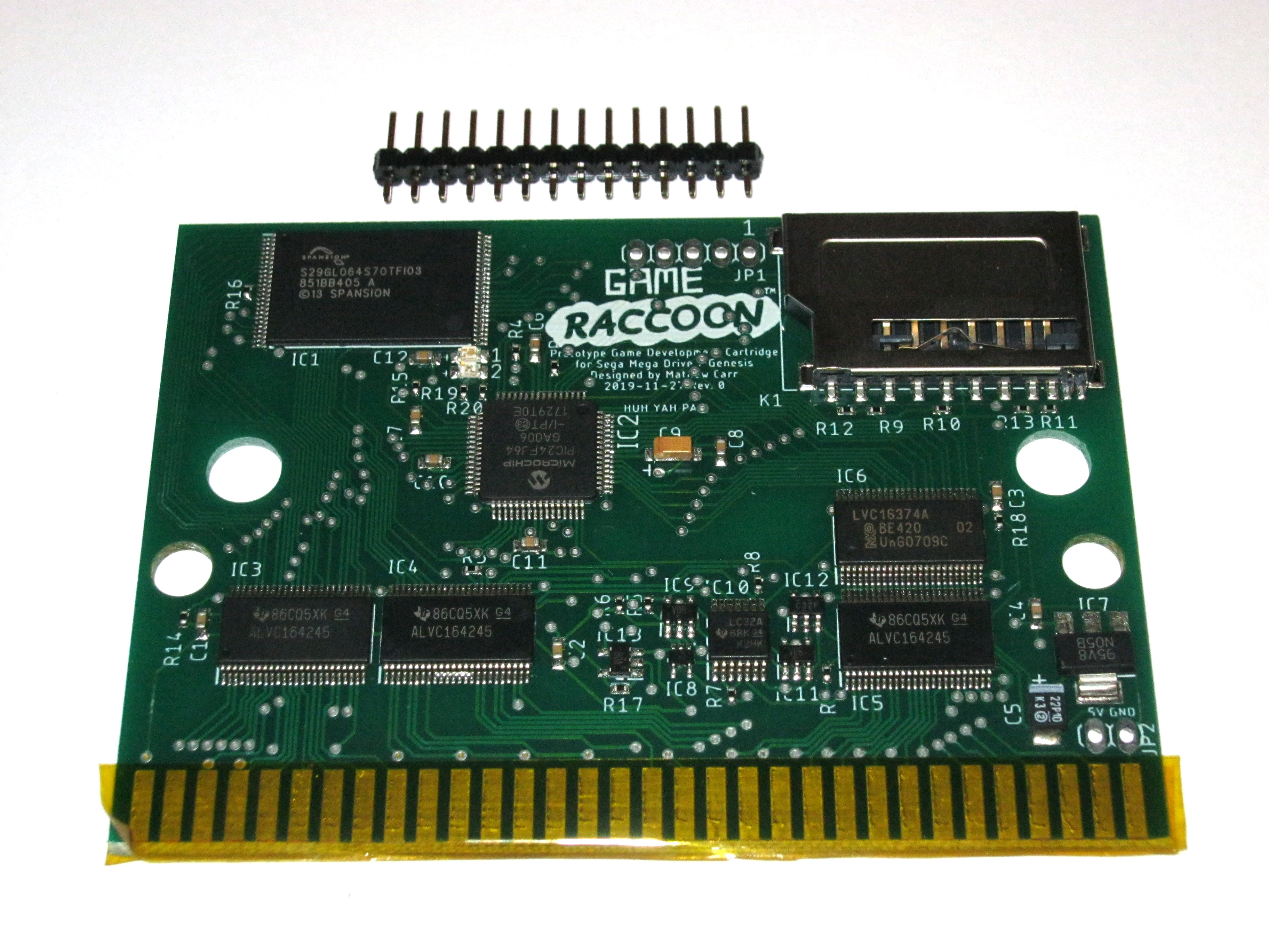
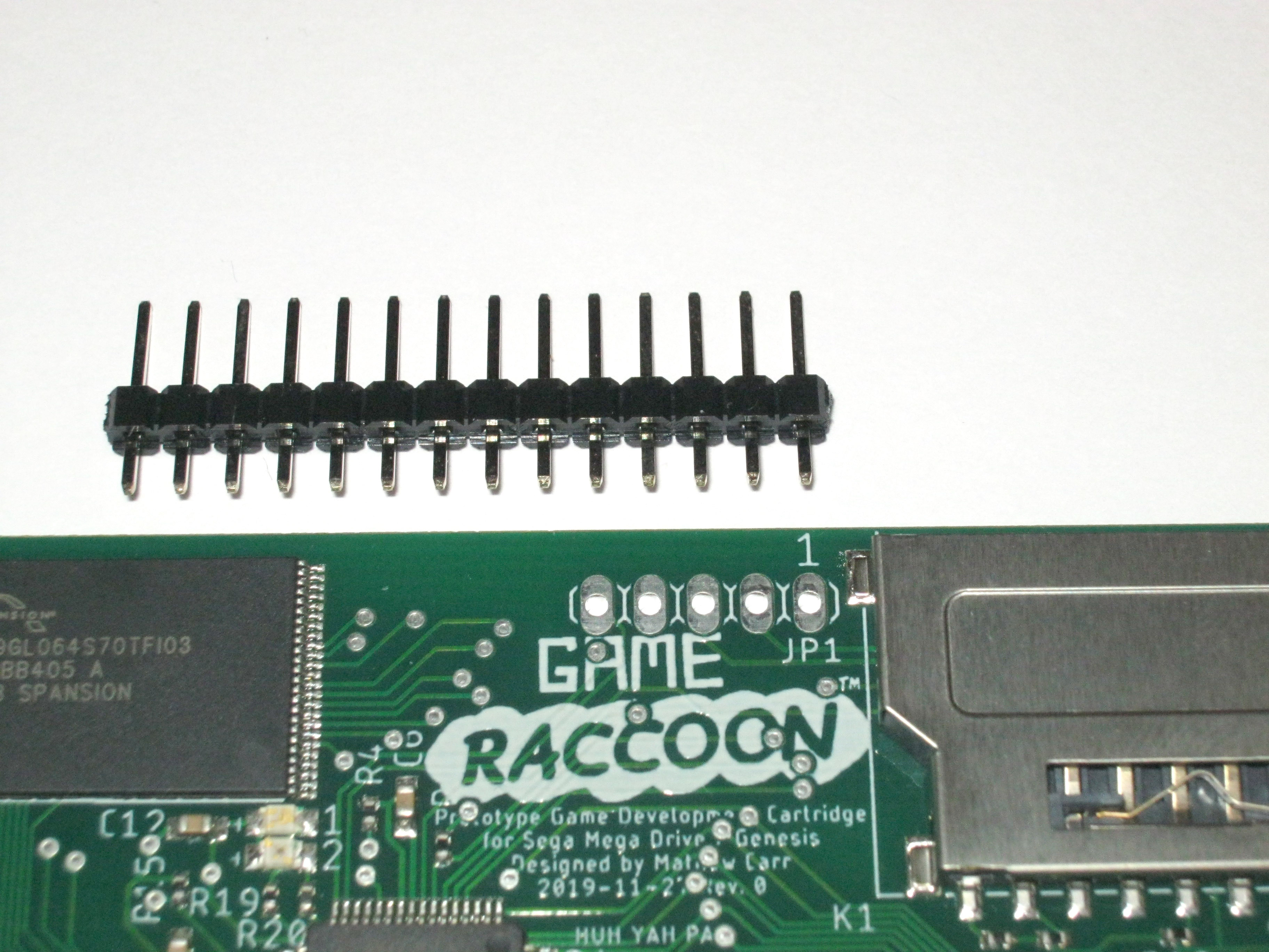
Here's a list of all the files in the FatFs project and the modifications I made to get it working with the Game Raccoon's PIC24FJ64GA006: • diskio.h - This file contains return value enums and function prototypes that collectively define the software interface that FatFs requires you to implement on top of the physical layer. I used this file unchanged. • ff.c - This contains FatFs' implementation of FAT. I used this file unchanged. • ff.h - This contains headers FatFs' implementation of FAT. I used this file unchanged. • ffconf.h - This contains configuration options for FatFs. I don't need write functions in the Game Raccoon, but I didn't edit this file to disable them yet. In the end I used this file unchanged. • ffunicode.c - This file contains huge tables and functions for converting and handling Unicode characters. I don't need these, and I don't intend to draw a complete Unicode bitmap tileset for the menu... however, there was no pressing need to remove this just yet. I used this file unchanged. • 
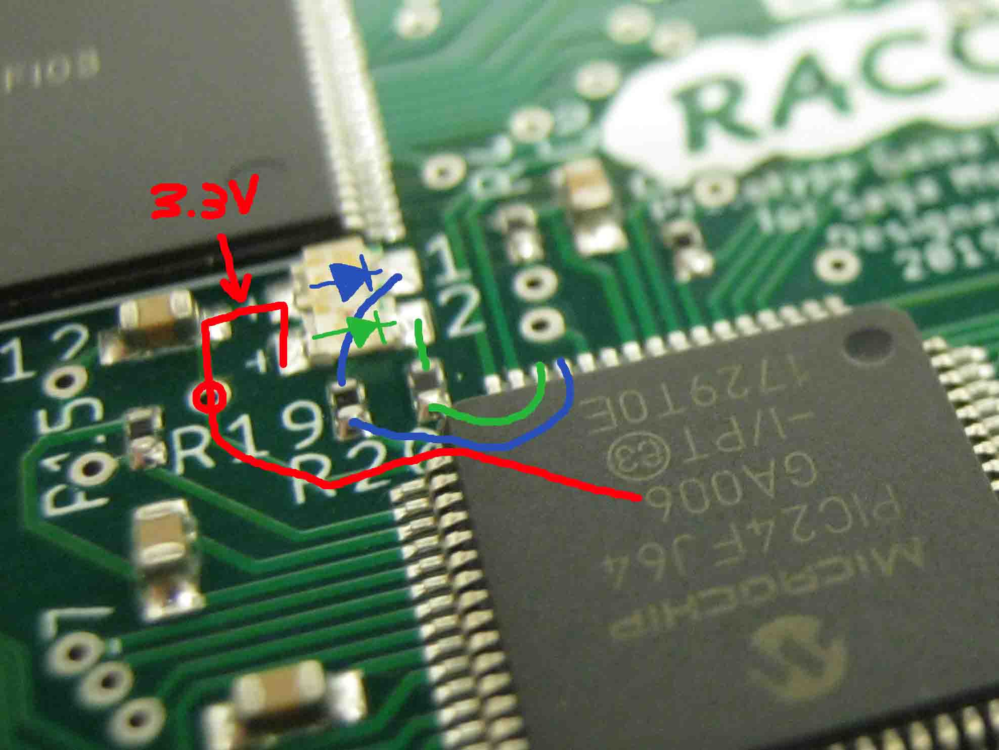
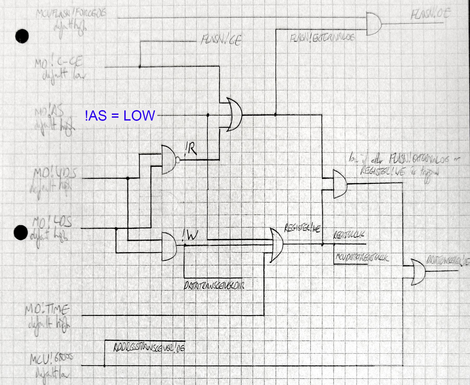
mmc_pic24f.c - Physical layer interface implementation for PIC24. The magic macro definitions used for memory-mapped variables in MPLAB X's headers have a slightly different naming convention to the one used by the sample project, plus my chip has a different set of peripherals, so I changed this file in a few places near the top: • • My version includes the generic Microchip header. • • CS_LOW() and CS_HIGH() macros required by FatFs to control the !SS signal to select SD card are changed to refer to the GPIO pin linked to SPI2!SS. • • MMC_CD magic macro variable returns the state of the card detection physical contact. Game Raccoon doesn't connect to this, so I force this to 1 for 'card always present'. • • MMC_WP magic macro variable returns the state of the write protection physical contact. Game Raccoon doesn't connect to this, so I force this to 0 for 'card always write-enabled'. • • FCLK_SLOW() and FCLK_FAST() macros are unchanged and still blank. I think these are to force certain PIC chips to dynamically underclock themselves to become compatible with SD cards temporarily. That functionality isn't needed here since I can configure the SD card SPI transfer rate in software. • • power_on() sets up the SPI channel for the SD card and enables it. I needed to set this to SPI2 and choose sensible clock prescale values. • • power_off() disables the SPI channel. • • xchg_spi() non asynchronously exchanges (sends) a byte with the SPI channel used by the SD card. I only needed to change this to SPI2. • • xmit_spi_multi() non asynchronously exchanges (sends) a byte series with the SPI channel used by the SD card. I only needed to change this to SPI2. • • rcvr_spi_multi() non asynchronously exchanges (receives) a byte series with the SPI channel used by the SD card. I only needed to change this to SPI2. • • The rest of mmc_pic24f.c is surprisingly unchanged! • main.c - I didn't use any of the code from the sample project's main.c as it wasn't necessary. In my own main.c I added the following: • • FatFs requires the function disk_timerproc() to be called at 1000Hz frequency, so I used Timer2 for this. • • And that's about it. The only other set up required to use the SD card is to call the FatFs external interface to mount the filesystem, etc. • pic24f.h - Preprocessor defines holding processor clock speed and macros for enabling and disabling interrupts used within FatFs. I use FCY in my code anyway, and I copied the macros into my main.c before other headers. I haven't looked into where these macros are called, but I assume they're necessary so I kept them. The rest of the files are specific to the sample project and I didn't need anything from them. • Makefile - Sample project makefile. Unneeded. • pic24sp.ini - Various configuarion for sample project. Unneeded. • picmmc.map - Various compilation object/symbol/map files. Unneeded. • picmmc.mcp - Various compilation object/symbol/map files. Unneeded. • picmmc.mcs - Various compilation object/symbol/map files. Unneeded. • picmmc.mcw - Various compilation object/symbol/map files. Unneeded. • pic_mmc.png - This is the above image. Unneeded. • tt.ini - Configuration options for the terminal program recommended by the sample project. Unneeded. • uart_pic24f.c - UART functions for the sample project. Unneeded. • uart_pic24f.h - UART functions for the sample project. Unneeded. • xprintf.c - Formatted text input and output routines for the terminal interface. Unneeded. • xprintf.h - Formatted text input and output routines for the terminal interface. Unneeded. 
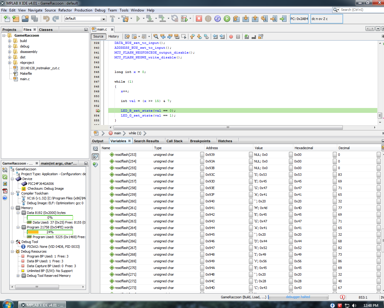
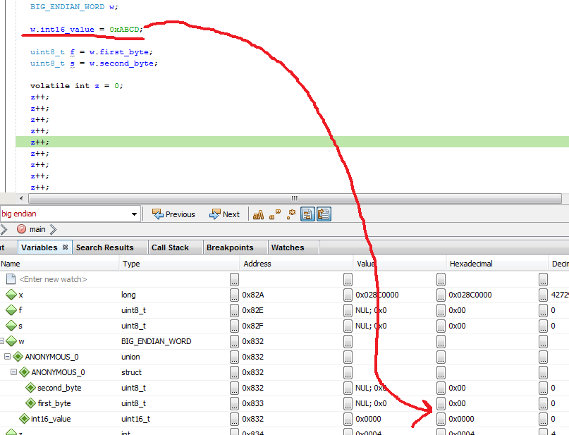
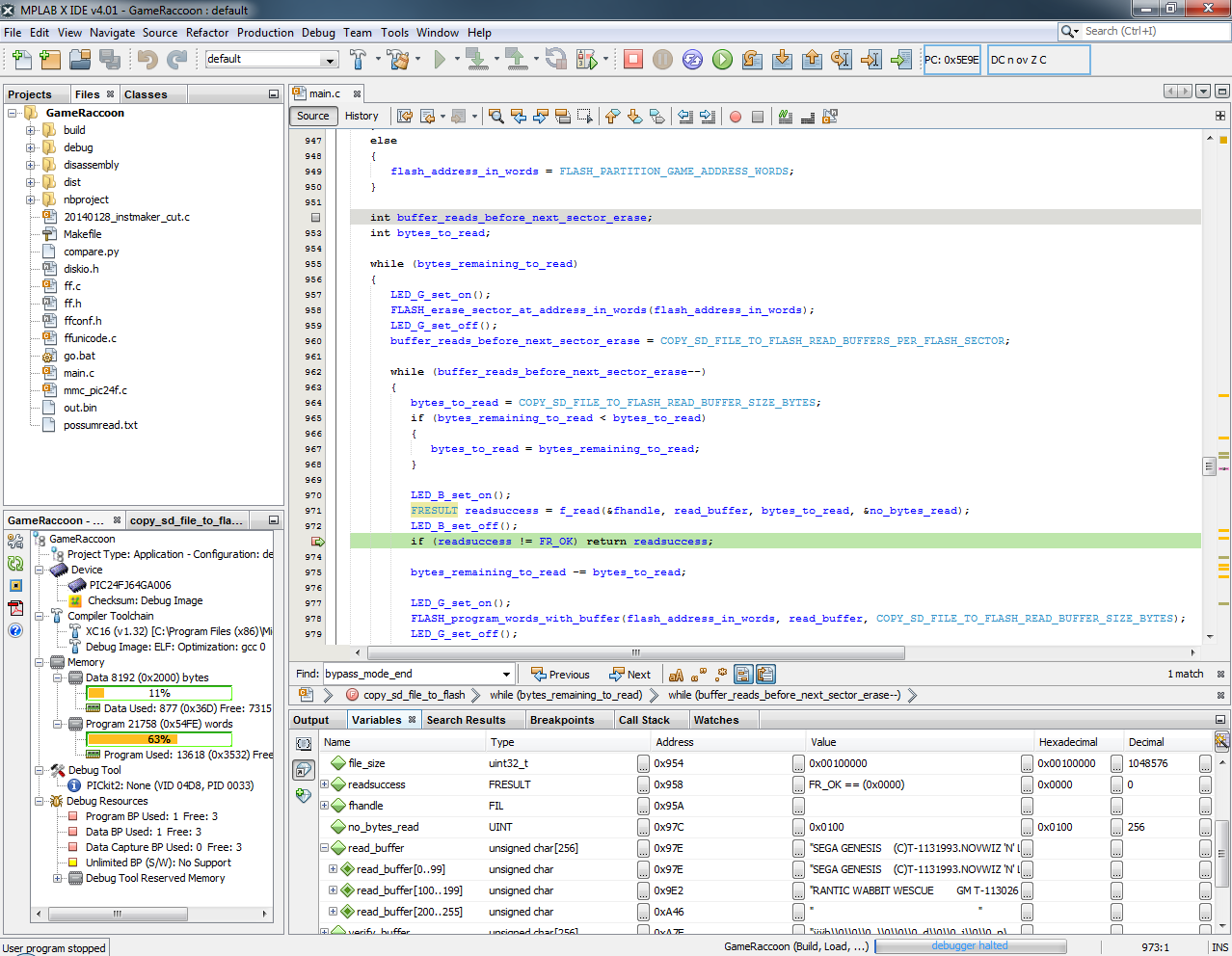
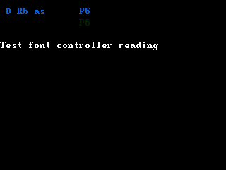
It was very surreal to be able to call the FatFs functions and see realistic data coming back. To slowly integrate FatFs' functionality into the Game Raccoon, I'd use one function at a time, stepping over its invocation in a debugger, watching the output variables and making sure each function did what I expected of it: f_open() on a valid path to a file should return success and give you a handle, f_size() returns the size, directory scanning with f_readdir() ought to populate the fname field with the currently identified item, and so on. I didn't have any problems with any of these. FatFs takes up over half the ROM space within the PIC, but that's exactly as expected. It's welcome to it, considering the amount of heavy lifting it's destined for. If I wanted (or rather needed) to reduce this, I could set the configuration flags to exclude write functionality, remove Unicode support, and so on. Sorry, Microchip, but you made no sense and I couldn't get you compiling. See ya later.

Mysteries of the Debugger, also Unions and Endianness

The debugger doesn't always play nicely... sometimes it'll just report phantom values that don't exist. That is really, truly unhelpful when I'm trying to see if I'm swizzling two bytes together in a union in the way that I expect. Here's another annoying things PIC processors do that will be absolutely meaningless to non-programmers: when you set a breakpoint in the IDE, you're selecting a line where you want the program execution to stop so you can inspect the current state of all the variables, and then slowly creep forward through the program to see what happens. PIC processors have a built-in problem called the 'skid effect'. (aka 'breakpoint skidding / slipping / sliding') https://microchipdeveloper.com/tls0201:skid-effect The Skid Effect means that when the breakpoint is reached, the processor is *already two instructions ahead* before it can be stopped. So say you had
password = enter_password()

if (password_is_ok()) {
 play_music()
} else {
 destroy_universe()
}
If you put a breakpoint on password = enter_password() to see if the password entry routine does something properly, it actually would barrel on ahead and probably destroy the universe. Every time I want to use a breakpoint, I have to put in half a dozen lines of useless code as a sort of runway for the processor to halt into. It's really annoying. The reason I'm using this union is because of the disconnect between the 'normal' C world of bytes and the Flash model of words. When I read bytes from the SD card, I'm reading a series of bytes as they appear in the file stored on the card. To write them to the Flash memory, I need to make them into an array of words, which means I need to be aware of the ordering that the 68000 expects. When the 68000 reads from address 0x0000, it's going to read the values that were stored in the first two bytes of the original file. The 68000 is big-endian, so if the first four bytes are 0x12,0xAB,0x34,0xCD, the value of the first word in ROM is 0x12AB. This means for each pair of bytes I read from the SD card, I need to put the first byte into the most significant byte of a word, and the second byte into the least significant byte.

Replacing the Flash

This is as good a time as any to mention something that I totally didn't intend, but instead just coalesced naturally as I redesigned the board and replaced the Flash. https://www.eevblog.com/forum/projects/designing-mega-drivegenesis-development-cart-m68000-interfacing-advice-please/ When I asked on EEVblog for advice, I was discouraged from using the S39VF6401B Flash module since the programming is word-only, and requires a slow command 'knock' sequence in order to disable the protection to get a single word inside it. You can see it in the topmost row of the left page, listed as 'Word-Program'. These are the pairs of values that need to be sent to the Flash for every single word that's sent to it. Since I'm manipulating the Flash with non-consecutive GPIO pins, outputting these values would be longwinded in the best case. As I said, I misread this advice and continued on with my plan. As it happens, I replaced the Flash module with another one for a completely different reason, and the new S29 Flash I chose because it was cheaper has a feature which greatly improves programming speed by removing the need for these long sequences. In the command guide in the right-hand page, it's version of the single word program sequence, 'Program', is exactly the same sequence as for the SST39 Flash on the left page. (I assume that there's some manufacturers' standard both Flashes adhere to to allow a baseline set of mutual compatibilities between different modules.) However, below it are commands 'Write to Buffer' and 'Program Buffer to Flash'. These commands allow the user to enter successive word writes into a 128-word buffer to be programmed all at once. This reduces the number of bus cycles by a huge amount! That's cool! You send 'Write to Buffer', which contains parameters for the buffer length and destination address, then send your values in consecutively, then end with 'Program Buffer to Flash'. Instead of 4 bus cycles per word, it's now 4 bus cycles to begin the buffer write, 1 bus cycle for each word to program, and 1 bus cycle to initiate the programming. A bus cycle in this instance is the time it takes to set 21 address bus GPIO lines, 16 data bus GPIO lines and set FLASH!WE twice. Considering that setting a single GPIO line is going to take at least 3 FCY to accomplish since I have to test a bit from a variable and set or unset a bit in PORT, that's (21+16)*3+2 FCY = 113 FCY = 7 us. To program 128 words with the old Flash, it takes 128 * 4 * 7 us = 3.58ms. For the new Flash it's (4+128+1) * 7 us = 0.93ms. Multiplying that up to the full 2 megawords (given that the maximum buffer size is 128 words) gives us: (2*1024*1024/128) * 128 * 4 * 7 us = 58.7 seconds and (2*1024*1024/128) * (4+128+1) * 7 us = 15.3 seconds. That's not a project-ruining difference, but it would be noticeable! Also, these are purely the programming times, the sector erasure times would have to be added on top to give the full boot or game partition programming duration. Also also, the new Flash has a mode called 'Unlock Bypass' which is a special mode you can put the Flash into that has shortened command sequences for the commonly used commands for programming and erasing the contents of the Flash. You can see the shortened sequences in the inset region in the middle of the table on the right-hand page. Using these shortens the partition programming time on the new Flash even further, though you have to make sure that you're entering Unlock Bypass mode correctly, otherwise the Flash will sit there silently and not erase or program at all, and you'll get very strange results when you read from it afterwards. So thank you bson for your evaluation. I followed your advice... accidentally... and it was a very good thing too. Related to the change in Flash module, but not a consequence of the available commands: in writing the Flash driver, the first hardware design flaw in the Game Raccoon quickly became apparent. Since the Flash erase and buffer program operations take non-negligible time, I have to introduce delays in the game programming sequence to ensure the Flash is ready before sending the next command. I first used a hardware timer set to wake when the maximum time indicated in the Flash datasheet for each kind of operation had expired. This worked fine to get things running quickly. I then tried to use the READY pin from the Flash to the PIC to query whether the Flash was currently busy. Unfortunately, I didn't pay enough attention to the datasheet and overlooked that this pin is open-drain on the Flash, so the connection is useless since I never added a pull-up resistor and so the pin is never pulled high! The toggle pin-polling approach still works, so that's what I use instead. The consequence is that I have to waste some time switching the TRIS data bus of the PIC from output to input to read the toggling value from the Flash and then back to output to perform the next action. It's not perfect, but the amount of time lost is negligible, so not having the READY pin available isn't devastating. I could use the timers instead of polling for toggles, but I've noticed that the Flash seems smart enough to know whether or not it needs to erase a particular sector (it probably has a microprocessor core in there that's more powerful than the Mega Drive itself...), so I'd waste time accommodating the worst case for each operation when the information that would let me proceed quicker is available. On the Ocelot, I use the CN weak internal pull-ups from the Change Notification functionality to detect the switch closed state on the joystick directions and fire buttons on the Zipstick/Sega Mega Drive controller port, and this would be the perfect scenario in which to use them to save the day! Except, not all the pins on this PIC support CN, and pin 39, to which FLASHREADY is connected, doesn't support it. Blast.

Testing the Game Raccoon: It's "Awesome!"

20th December 2019: Here we go! FatFs is compiling without any complaints, and I'm able to open up a file with f_open() if I explicitly name it as a string constant, and measure its size. You can see how much of the PIC's PROM space is taken up by FatFs in the project explorer in the lower right. Most of that is the Unicode conversion tables, I think. Alright! I'm reading the bytes 'SEGA GENESIS' at 0x100 from the SD card! That means the reading from SD card is working fine. It's pretty convenient that these strings are ordinary ASCII, huh? If you see something that looks similar to 'SEGA' but is shifted up or down a few characters, then you ought to check all your #defines that map the physical pin PORT and LAT memory-mapped IO to logical names - I was getting some mis-written data at one point, and it was because I'd skipped over a line when I was copy-pasting and modifying my list of PORTs and LATs so one pin wasn't being set correctly. I'm integrating this into a loop which erases Flash blocks as it goes, reading chunks of data from the SD card sized to fit the Flash programming buffer, and passing this to a function which performs the necessary swizzling and GPIO outputting to the Flash module. It all seems to be rumbling along, erasing blocks and filling them up with the contents of Wiz 'n' Liz like a well oiled machine! Either that or it's all failing together in a consistent way... it's possible the bytes are being written in the wrong order, but there's only one way to know... As much as I like Wiz 'n' Liz, to properly test the Game Raccoon, we need a game that has good, clear graphics; interesting sound (preferably lots of speech and samples); and a recognisable intro sequence that I don't have to press any buttons to get to. In short, we need Awesome Possum Kicks Dr. Machino's Butt. I'm going to write it to the boot partition of the Game Raccoon and see what happens when I put it in the Mega Drive. If my calculations are correct, the default behaviour of the Raccoon will make the Mega Drive boot from the first 4 megabytes of the Flash module as if it were an ordinary mask ROM, hence booting my image of Awesome Possum. Hang on a moment, that's a point. I need to write a firmware to the PIC so that it'll immediately go into an infinite loop and do absolutely nothing to the control signals; leaving them in their default 'boot from boot partition, PIC idle' state. If I leave the current firmware in there, it'll isolate when power is applied, while the Mega Drive is trying to boot from it! That would be very bad. Here it is! Awesome Possum Kicks Dr. Machino's Butt's glorious opening chorus, as played by the Game Raccoon Revision 0. I chose Awesome Possum because of this long opening chorus - if the logic was faulty, then the sequence wouldn't play, or the graphics would be corrupted or the audio would be glitchy. As you can see, it's stable and clear. Unfortunately, past this point things go awry. (Ignore the background music, it's supposed to sound like that.) You may have noticed a flaw in the cinema magic here, when my sinister, ghostly reflection has to reach forward and press Reset on the Mega Drive to start the game. This strange behaviour is to do with powering up the Raccoon I think, and transceiving !VRES and connecting it to the PIC and Flash with a pull-up resistor. When the Mega Drive is powered on, sometimes the Game Raccoon will show a fully blank screen. The first thing the Game Raccoon Revision 0 boot ROM does is satisfy TMSS, so it should be displaying the PRODUCED BY OR UNDER LICENSE screen. If you press the Reset button on the console while powered on, the cart boots normally. I'm not sure why this is. My thought is that perhaps the regulator and capacitors I'm using are causing the cart to not be fully stably powered by the time the 68000 comes out of reset and begins demanding data from the 'mask ROM'. Alternatively, my passing of !VRES into the cartridge might have either the PIC or Flash or both not available in time. As you can see, it works eventually so I'm not going to think too hard about it just yet. It's a quirk. :) What isn't working in Awesome Possum: • Alphabetical characters on the prologue screen and level card. Strangely, the comma and numbers work. • Background tiles during gameplay. • The left and rightmost animals during the quiz. All of these things are showing up as solid blocks of a single colour.

Why are all of these things showing up as solid blocks of a single colour?

A good question. To fully explore this, I'm going to have to test multiple game images and see how they react to be being played from the Game Raccoon hardware. I could manually burn images into the PROM by hard-coding a filename into a temporary firmware like I did with Awesome Possum, but that's going to get old fast when I'm trying many different images. It's time to write the menu!

Writing the Game Raccoon software

I need to test the Game Raccoon with more games, and the easiest way to do that is to crack on and write the handshaking protocol, menu software, SD card listing, game installation process and booting. Lots of interesting low-level stuff to get on with. Alright, I know what I need to write, but before I can get started on the actual code, I need to get myself a 68000 assembler! I've written 68000 code a few times before: the original Gravity Beam for the Commodore Amiga 500, and my YM2612 Mega Drive Instrument Maker. Both times I used an assembler called vasm, and the exact version is in my backups... somewhere. (It's always a good idea to back up your entire work environment, keeping all your weird tools together, whenever you back up a project!) For some reason Windows builds of vasm are difficult to find, which is annoying. I recall I keep having to find third-party builds from random folks and hope they don't annihilate the universe when I run them. I've got a shiny... old?... copy of vasmm68k_mot_win32.exe here. Let's do it! vasm 1.7d (c) in 2002-2015 Volker Barthelmann vasm M68k/CPU32/ColdFire cpu backend 2.1 (c) 2002-2015 Frank Wille vasm motorola syntax module 3.8a (c) 2002-2015 Frank Wille vasm test output module 1.0 (c) 2002 Volker Barthelmann Everything seems alright there. So, where to begin? Easy. We cheat. I'm going to get the source code for the Instrument Maker and get that compiling first. I'm going to continually, incorrectly and inconsistently use 'compiling' rather than 'assembling' throughout this since it rolls off the tongue easier. To me 'assembling' sounds like I'm pushing a bunch of boxes together to put them in the same room, whereas 'compiling' sounds more softwarey. One thing that probably isn't obvious to anyone who hasn't used it before, but the executable you get of vasm dictates what syntaxes it supports, and you can select an output type using command-line switches. For Mega Drive projects, I want the output to be raw assembled 68000 binary machine code, without any headers, wrappers or symbolic information. The Mega Drive expects to find the entry point of the cartridge software at the memory location stored at address 0x4. To get binary output, use the switch -Fbin. When I was doing Gravity Beam for the Commodore Amiga 500, I didn't want raw binary output - I relied on vasm (or the toolset of which vasm was a part) to perform the correct magic necessary to produce a complete AmigaDOS compatible, Workbench-1.3-safe executable. I believe the file format for this is a 'hunk'; you can read more about this in the vasm documentation, and in the Gravity Beam make scripts in the source .zip. It worked. :D The Instrument Maker source code contains everything one needs in order to get a Mega Drive-compatible binary image generated, together with a bunch of other random stuff, some useful, like the controller code, and some not. What I want first of all is a completely empty image that satisfies the TMSS check and then loops on a completely black screen. I'm going to take out as much as I can, leaving it with just the macros necessary to populate the Mega Drive header and satisfy TMSS. You know, I've kinda completely forgotten how everything in the Mega Drive's VDP works. I was never really that knowledgeable about it, since all I did in the instrument maker was put up a background. I guess this is gonna be exciting. My memory is saying that the VDP contains its own memory, like the corresponding chip in the Master System, and there's a special I/O-related way to get the data inside. This means that whenever I want to change the contents of the tiles or change which tiles are displayed on the screen, I'm going to have to do some numerical gymnastics to do so. Like most embedded or early console projects, the instrument maker source begins with a huge block of defines and macros that assign (barely) nicer names to all of the important memory locations in the Mega Drive where all the peripherals live. To be a valid Mega Drive image, it has to begin with the 256-byte Motorola 68000 vector table, followed by a 256-byte Mega Drive-specific header. This header is going to be populated by a big rectangle of constant declarations in the assembly source code. There's nothing here that's difficult or needs to be generated - the Master System BIOS checks checksums, but the Mega Drive doesn't. According to the various reverse-engineered docs I'm reading, the only part of the header that needs to be present is the characters SEGA at a specific position, which I imagine could also be satisfied if your image contained something like MOUSEGAMES there. This also brings to my attention something I hadn't considered up until now: the interrupt vectors live in the ROM and can't be changed. Unlike the C64 where the interrupt vectors live in the highest part of the memory space but can have RAM banked in on top of them, the Mega Drive's interrupts live in the lowest part of the address space, which is typically mask ROM, but is in my case the Flash PROM. The consequence of this that when the PIC isolates the cartridge, the Flash will become unreachable and the contents of this table will become indeterminate, causing complete havoc if an interrupt occurs while isolation is active. On top of that, none of these garbage vectors will be valid addresses anyway! All the bits ought to be indeterminate, except the lowest bit, which my pull-up resistor will force to 1, which in turn will make all the vectors into invalid, non word-aligned addresses (this is indeed how we'll check for isolation on the Mega Drive side!), so it'll cause an Address Error exception, and the attempt to jump to the appropriate vector will cause another Address Error exception, which will halt the processor completely. In short: before I write to !TIME and cause isolation, I must disable interrupts first! The safest thing to do is to have the Game Raccoon menu firmware never have interrupts active at all, if that's possible. The only interrupt I'd use in the normal course would be the vertical blank interrupt, but there may be other ways to detect that. There's so many defines and things in here, it's hard to find the real entry point of the cartridge! Here's some random VDP docs for the Mega Drive. I flick between these constantly, since no single one of them seems to explain what I want to do in terms I understand. https://segaretro.org/Sega_Mega_Drive/VDP_general_usage https://megacatstudios.com/blogs/press/sega-genesis-mega-drive-vdp-graphics-guide-v1-2a-03-14-17 https://darkdust.net/writings/megadrive/firststeps http://jiggawatt.org/genvdp.txt https://plutiedev.com/mirror/kabuto-hardware-notes Getting the screen to black was simple, but now I need to put something on it! I'd show you a screenshot, but, well, it would be completely black! I need some graphics. I need a font!

I need a font!

I used the font I drew for Gravity Beam in the Instrument Maker since it was there, but I'd like a nicer font for the Game Raccoon menu. Something clear and distinct. I could draw my own, or I could follow the lead of my good friend Tomstein and look at OpenGameArt. OpenGameArt is a repository for game assets (such as graphics, fonts, music, tiles, sprites, and so on) that are licensed under permissive or copyleft licenses. Here, I can search for assets by tag or title (say, 'font') and license. It has checkboxes for various Creative Commons and GPL license variations; if I want a font that I can use for any purpose with only attribution required, there's CC0. Here's New original Grafx2 font collection by usr_share: a collection of bitmap fonts all licensed under CC0. Perfect. I really like the TrioDX and TrioDX2 fonts at the bottom there - they remind me a lot of the dialogue in Shining Force, though the 'DX' name makes me think they were aiming for Link's Awakening DX. To use it in my menu, I need to convert it from a .png into a nice squished-up-yet-easily-readable format that I can push into the VDP using some 68000. The characters themselves form a 1-bit, 8x16 font, but if you look at this zoomed in image, you can see that each letter is padded with one pixel to the left and above; with a marker notch pixel in the corner to separate out each character. I'm going to write a Python script that copies out 8x16 rectangles from this .png, does the necessary re-encoding, producing a binary file, storing each line of a tile as a byte. It's a good idea to check the size of the resulting file to make sure you haven't lost any characters or sheared something along the way: 8*16 bits / 8 bits per byte * 94 printable characters (I didn't use the 'cx' character) = 1,504 bytes. The next step is to include this binary file in the Game Raccoon image and get it into the VDP. This means I have to 'decompress' it back into a 4 bits-per-pixel tile graphic on the fly and tell the VDP to write these new words into the VRAM. With that done, I can now put tile indices onto one of the playfields and get some words on the screen. Or, rather, I have to write a palette first, but then I can get some words on the screen!

Words on the screen, and controller reading too

I thought my old Mega Drive controller reading code was good, but it started acting very strangely in some of the emulators I used. I was going to review the code I'd written against the reference I used, but I'd been out of touch with the Mega Drive 'scene' for so long that the main site that I used for reference had long since shut down! :( (there was md.squee as well another wiki that had a similar logo, both are gone now it seems) However, I found this new guide: https://github.com/jonthysell/SegaController/wiki/How-To-Read-Sega-Controllers And I was surprised to find that their description of the stages and some of the button mappings were all sheared compared to my own. I was leaving my TH pin in a different state to theirs, and our numberings didn't correlate. When I programmed the 6-button Mega Drive loading code for the Ocelot Arcade system, I copied it from the Instrument Maker, and found I had to swap some buttons there too, so finding that I'd made a mistake wasn't entirely unexpected after all. I rewrote my 68000 controller reading code according to that guide, and everything was funky lovely. The letters you can see in the image above are the currently depressed buttons. The 'P' and '6' refer to 'Controller Present' and 'Six button controller', which are both states you can determine from reading the two controller ports.

What emulators are you using, Matt?

All of them. They all have different strengths and weaknesses, but ideally your image ought to work in all of them! Fusion is the typical emulator you'd use for playing games. For capturing video, I'd use Bizhawk since it's reliable and accurate and has a nice facility for recording lossless video. For debugging, I tried Regen, which crashed all the time; BlastEm, which I couldn't figure out; and Exodus, which crashes somewhat less, but... It's definitely designed for a multimonitor setup! Exodus has a strange workspace system which lets you dock and undock almost every pane however you please. From left to right, I've got: • Register values so I can see what the 68000 is thinking. • Disassembly so I can see what's being executed. I have to constantly manually tell it what address to disassemble from. • RAM viewer/editor so I can see what's stored. • Breakpoints so I can pause on execution of certain addresses. You have to have this exact window (perhaps a specific input widget) focused for the step keyboard buttons to work. • VRAM viewer/editor: • Plane viewer showing the full, non-scrolled tile fields. • Palette viewer showing all the palettes. • Video output. What I can't figure out how to do is to force the output to be integer pixel scaled. That would be really handy. :( Being able to set breakpoints is very very useful, but I'm still loading images and doing tons of stuff the old fashioned way. I don't have any of this integrated with the editor I'm using for code. I'm using Notepad++ to write the 68000 code, and I don't even have a 68000 vasm highlighter installed - I suppose I really ought to get one. Writing to the palette is a surprisingly big fuss on the Mega Drive. If I'm understanding correctly, the VDP can be accessed through a pair of addresses referred to as the Data and Control port. Each of these are word-sized and followed in the memory map by a mirror of themselves. Except the register behind the Control port is actually longword sized... I think? Most operations you'd want to perform on Mega Drive graphics can be achieved by a word-sized write to the Control port, setting the address in VRAM upon which the next operation will act. This is except for operations on sprites and palettes, which require the longword version to set some upper bits that hold some VRAM destination flags. Once you've finished messing with sprites or palette entries, you have to perform another longword write to clear the flags, resetting the VDP back into 'word-sized address writes are ok' mode. I think it would make more sense overall if I just stuck to longword writes to this register at all times, so I'm always in complete control of what VRAM write or read mode is in effect! It took me about three hours to get text on the screen, and that was 10 minutes setting up the project and importing the project, and two hours and fifty minutes trying to write entries into the palette.

Directory cache stuff

It's time to define how I'm going to generate the game list by interrogating the SD card with FatFs in C on the PIC, store it on the Flash within the boot partition to share it with the Mega Drive side, and parse and display it within the 68000 assembly Game Raccoon menu. Originally, my plan was to store all the files in the root directory of the SD card and ignore directories completely. The user would select the index of the file in the directory listing and write this to !TIME to select the game. A few weeks later, when I was planning the !TIME sequence, I wrote that I could have directories easily, without introducing any more complexity to the system. If I include directories themselves in the linear list and group the contents of a directory contiguously, I can flatten the directory tree into a linear list in a very straightforward manner. I call the resulting list of directories and their contents together the 'directory cache'. Each record in the directory cache is a fixed length, which greatly simplifies programming on both sides (C and 68000). I picked 256 since it's a nice round arbitrary number that ought to be suitable for almost all pathnames that are likely to be encountered. I've put it at the half way point of the boot partition: also arbitrary, but it'll do for now. Allocating half of the 4 megabyte image to 256-byte-long records gives enough space for 8192 records, which is more than enough. All these values are subject to change if I need more space in the boot partition for assets to make the menu look more nice (more than 2 megabytes? That would be incredibly extravagant!), or if I expand the directory cache record length to store more data about the items. The smart thing to do would be to write a series of programs to simulate the process of interrogating a folder and generating the directory cache 'offline', and write the menu system to inspect these generated simulated files. Of course, I was a risky sod and did it the other way around: getting it to work on the hardware first, and then writing a simulator afterwards. I went through a couple of iterations of designing the system, but in the end I came up with this: The directory cache contains a list of the full contents of the SD card. It is regenerated whenever the magic number $FFFE is sent to the !TIME register. Currently this happens every time the Game Raccoon is powered on - the final firmware would allow you to do this on-demand. (Or not, if you're certain the SD card contents are unchanged.) The directory cache consists of a series of records indicating either a directory a file. Records (or nodes if you prefer) are linked together in a tree structure. The first item in the directory cache is always . representing the root of the SD card. Both directory and file records begin at offset $00 with a $00-terminated full pathname of the item. Directories do not have a trailing slash. Directory items have four uint16_t fields located at offsets $F8, $FA, $FC and $FE. $F8: Number of directories D in this directory. $FA: Number of files F in this directory. $FC: Record index containing the start of the list of contents of this directory. $FE: Record index of parent directory. (This is 0 for the root.) The contents of a directory are located at the record index indicated by $FC. This is always a contiguous list of D records for the directories (if any) followed by F records for the files (if any). File records consist of just the $00-terminated full pathname beginning at $00. This means that the maximum pathname to a file can be 255 characters, and 247 for directories. Since the directory cache lives in the region $200000-$3FFFFF, it can hold 8192 (including both directories and files). However, testing these limits is very unwise. :D python imitate_directory_cache.py can be used to create a directory cache offline. This reads a local folder and makes an imitation directory cache as if it had come from the PIC in a real Game Raccoon to be linked into the Game Raccoon boot ROM binary for testing in emulators. python directory_cache_read.py friendly prints the contents of a directory cache data block. For example: 0: (3,2,1,0) . 1: (0,3,6,0) ./freeware 2: (0,10,9,0) ./homebrew 3: (0,3,19,0) ./demoscene 4: (0,0,0,0) ./YM2612maker.bin 5: (0,0,0,0) ./TANGLEWD_demo.BIN 6: (0,0,0,0) ./freeware/wiznliz.bin 7: (0,0,0,0) ./freeware/Zero Tolerance.md 8: (0,0,0,0) ./freeware/Beyond Zero Tolerance (prototype).bin 9: (0,0,0,0) ./homebrew/RetailClerk89_2019-08-18.bin 10: (0,0,0,0) ./homebrew/Airstriker.bin 11: (0,0,0,0) ./homebrew/ULTETRIS.BIN 12: (0,0,0,0) ./homebrew/SegGalaV0.06.SMD 13: (0,0,0,0) ./homebrew/omega_blast.bin 14: (0,0,0,0) ./homebrew/MegaAtoms.bin 15: (0,0,0,0) ./homebrew/PRINGLES.BIN 16: (0,0,0,0) ./homebrew/Misplaced-EN.bin 17: (0,0,0,0) ./homebrew/Uwol_Quest_For_Money.bin 18: (0,0,0,0) ./homebrew/OldTowers12.bin 19: (0,0,0,0) ./demoscene/TiTAN_Overdrive.bin 20: (0,0,0,0) ./demoscene/fullscreen_niccc2000.bin 21: (0,0,0,0) ./demoscene/TiTAN_Overdrive2.bin Consider the root directory 0: (3,2,1,0) . The first number before the colon, 0, is the record index. This isn't stored in the cache and is implicit in the address of the record in PROM. The 3,2,1 means that there are three directories and two files, found starting at record 1. Adding together three and two gives five, the total number of items contained in the root directory. The final 0 means that the parent of this directory is record 0. This means that if you were to try to ascend from the root, you'd not change directory. (Note that menus and so on detect that you are in the root by checking that the current record index is 0.) If we look at the list starting at record index 1: 1: (0,3,6,0) ./freeware 2: (0,10,9,0) ./homebrew 3: (0,3,19,0) ./demoscene 4: (0,0,0,0) ./YM2612maker.bin 5: (0,0,0,0) ./TANGLEWD_demo.BIN Using the D and F values from the root directory, we know that the first three items ./freeware, ./homebrew and ./demoscene are directories and the next two items ./YM2612maker.bin and ./TANGLEWD_demo.BIN are files. Notice how the directory cache list when printed in linear form is a very straightforward array. Specifically, since the filename strings are always present at offset $00, then address $200000 + $100*index is always a pointer to the fully qualified pathname of item index. When the user selects a file from the Game Raccoon boot ROM menu, it's the record index that is written to the !TIME register. On the PIC, this is used as an index into the Flash ROM's directory cache to retrieve the full pathname to pass into FatFs' f_open(). When a directory is selected, the record index number is set as the current directory and the menu is redrawn with no communication with the PIC. When the menu is printed to the screen, only the filename part before the last forward slash (if present) is printed. Notice that the directory cache contents aren't sorted. The PIC writes the entries to the directory cache as they're reported by FatFs' f_readdir() function, which in turn is the order that they appear in the filesystem, most likely the order that the original file entries were created on the card. The PIC doesn't have the RAM to sort these, so they're written unsorted. When they're navigated to by the Game Raccoon menu, they're sorted by the 68000 (or rather, a list of pointers to record indices are sorted) when the menu reads the list of items in the present directory. It would be possible to sort the files on the PIC if a binary tree was built as the entries were read, and then when the tree was complete, the necessary pointers to allow an in-order traversal without a recursive algorithm were written (or the 68000 was told how to perform one recursively). A very useful end result of storing the full filename is that the filenames in the directory cache aren't at all linked to any part of the FAT filesystem on the card, so if, for some reason, the files are moved physically on the drive geometry, the directory cache would still work. If the SD card were removed and some files added, then any part of the directory cache that refers to files that still exist would still function normally. If there is no file at the given pathname on the SD card, the Game Raccoon will lock up in isolated mode with the LEDs flashing to indicate an error. This isn't especially pretty, but it shouldn't happen unless you've done something very inadvisable.

Assembling the complete image with fruitsalad.py

How is the Game Raccoon image assembled, anyway? (Notice how I've switched to 'assembled' here, since I'm constructing the final 4 megabyte Game Raccoon menu image to be written to the boot partition out of individual pieces that all slot together like bricks in a wall.) The generation of the image is controlled by a Python script called fruitsalad.py (named so since it chops up files into little pieces). "generate_included_binaries_blob" - Using a list of filename-symbol pairs, create a binary blob included_binaries.bin containing all of the files from the list, longword aligned, together with assembly source file included_binaries.68k.asm containing their start and end address and length if the binary blob were to be located at $200 in the Mega Drive memory map. • "compile_ramresident" - Assemble the Game Raccoon main RAM-resident code with origin $00FF0000 into binary file raccoonramresident.bin, using the calculated offsets from the above file to locate binary data in ROM. • "combine_entry_point_ramresident" - Create the Game Raccoon boot image file by compiling the entry point stub source asm, which incbins the included binaries blob into $200, and the compiled RAM-resident binary into ROM following the entry point stub. This is the complete Game Raccoon boot image, except without any directory cache present. • "append_imitation_directory_cache_binary" - Create a faux full 4Mbyte boot partition binary by combining the bare Game Raccoon boot ROM image with an imitation directory cache (created by imitate_directory_cache.py). You need this to test the Game Raccoon boot ROM on an emulator since there wouldn't be any directory cache otherwise. • "complete_boot_rom_image" - Target that executes all of the above in order. The reason why this madness is needed is because there's no simple way to ask vasm to change the current assembly address. In the assembler I'm using for the C64 (the one that comes with C64Studio), you can assign to the asterisk * to change the current working address. In vasm there are some directives that can change the working address, but only forwards, and a jump always results in the skipped bytes being included in the binary image. This means I can't change the working address to $FF0000 to generate code targeted at the Mega Drive's RAM without creating a huge file (if I wanted to compile both the entry point and the RAM resident part in one file). Yet, vasm allows you to set the assembly address to a higher one without introducing padding if there hasn't been any prior output. Therefore, I have to compile the binary sections separately and insert all the independent parts into the sandwich when compiling the entry point stub part. It works. :)

!TIME enough at last

It's the correct moment to discuss the usage of the !TIME register. You may think that my masterplan was full of invisible issues waiting to render my cartridge useless! The fact is... Everything worked first attempt. There's the code. It does exactly what I said it would. TIME_write writes a word to the Game Raccoon communication register. The caller must expect the cartridge to be isolated very shortly after calling this macro, and for isolation status to not be stable enough to allow the 68000 to check for a short duration afterwards, so a short loop is used to enforce a delay for now. After this duration, the macro GAME_RACCOON_isolation_test can be used to populate the Z condition flag with the current isolation state. If Zero, isolation is not in effect. If Non-Zero, isolation is in effect. The mechanism works by reading and testing the lowest bit of the longword value of ($000000), which is the initial value of the stack pointer as stored within the 68000 vector table. The middle fragment of code shows one simple use of the two macros to send a message to the PIC through the communication register mapped to !TIME, and wait for isolation to end. This is used in the Game Raccoon menu after TMSS to wake up the PIC. It is only necessary to wait for deisolation if the 68000 side wants to read any value from the PROM of the cartridge or to send another !TIME. Since the Mega Drive is executing from RAM at this point, and all the graphic tiles ought to have been copied into VRAM, it would be possible to play animations or music during isolation while the cartridge is busy. Care must be taken to not accidentally attempt to read any constants from PROM: it would be easy to forget and try to read some strings stored in a table in the included binaries blob in PROM. Anything the Mega Drive 68000-side code needs to refer to during isolation needs to be RAM-resident, including strings and tables! Conversely, anything that the RAM-resident code doesn't need to refer to during isolation should be included in the binary includes section. The code at the bottom is the boot sequence for launching a game from the Game Raccoon menu. There's nothing to say about it: it sends the launch command to !TIME, (the PIC changes MCU!BOOT/GAME to 1 to switch the Flash to the game partition), waits for deisolation, then loads the two values from the header of the loaded image then jumps to the value in the entry point vector. I took this screenshot to demonstrate how my typical assembly language code looks. The assembled version of what you see on this screen adds up to about 70 or 80 bytes total, which is about a third of how much it takes to store the contents of this paragraph. I am a sucker for super long label and variable names. The directory cache is populated in the order that f_readdir() returns the entries, which I assume is the order that the surviving file entries were generated in the FAT on the SD card - if any files were deleted, renamed or written in a non-alphabetical order, then the resulting list would be random, much like how dir would display the contents of a directory out of order by default in MS-DOS. (I remember my Great Uncle having a strange tool, possibly from Norton or Quarterdeck, whose job it was to alphabetise directories... madness!). To display the contents of folders in alphabetical order in the Game Raccoon menu, the contents of a directory cache record folder are sorted when the directory is selected. The addresses of the names of the files (or folders) within a folder can be found at $100 offsets from the base contents record index number of the selected directory. Once these have been identified, all that's left is to sort this list of string pointers in place. Amazingly, my sort routine worked first time, which is pretty good for somewhat rusty 68000 code, I think! Though, like a buffoon, after taking this screenshot and showing it online, I only realised a good while later when I was fixing some menu mysteriousness that in copy-pasting the 'iterate through directories and sort them' section, I didn't realise I'd reused DIRECTORY_CACHE_OFFSET_TO_DIRECTORY_COUNT in the file loop, so it was reading and iterating through the number of directories when it was supposed to be iterating through the number of files. Needless to say this caused explosions, but thankfully only the theoretical kind.

The menu is done, more or less!

It's not pretty, but it is functional. There were a couple of false starts, some silly mistakes here and there, and the whole thing is held together with wishful thinking, but it's enough to navigate the directory cache and select items from the SD card. In this version, the Game Raccoon automatically requests a directory cache refresh every time it's powered on, directly after the handshake. This isn't the behaviour I wrote in my design, but it ensures that the contents of the cache are always valid, and I don't have to mess about putting in an option for it right now or dealing with invalid menu items. You get a medal if you know why it has the silly caption that it does.

Of all the cruel damned tricks...

Yeah, that's right. Of all the things to work: Bubsy II. Not even the first one, just Bubsy II. Though, if you look close you'll see that the life indicators don't work. I haven't a clue why only those aren't working, yet the rest of the game looks fine. I suppose it makes sense. The more technically accomplished a game is (typically the later it is), the more it relies on DMA for fancy things. Overdrive is entirely invisible, whereas Bubsy II is entirely visible.

Alright, so why ARE all of these things showing up as solid blocks of a single colour?

At first I thought that the PIC's copy operation from the SD card to the Flash was faulty - as if there was a block of $FF being written at some point in the ROM image where the graphics ought to be found. I tried to reproduce this effect in an emulator by overwriting parts of Awesome Possum with $FF, but I couldn't. Replacing large chunks of the end of the image with $FF to simulate the effect of the copy being interrupted part way through (as if the file size was being reported incorrectly by FatFs, or the SD card was browning out due to the power-inline resistor) had no effect except making the game not boot at all eventually. Tests with some other software showed that it was only ever graphics that were affected, backgrounds in some games, sprites in others (such as Ecco: The Tides of Time, where Ecco becomes a lovely, fluid... mass of squares, and so does Blaze in Mobius Evolution and I expect other Sonic 1 hacks), HUD elements in others. Anything else, such as music, sound effects, samples and gameplay are all uninterrupted and perfect. For some reason, I believe certain graphical elements are being copied into VRAM as $FF. The next likely candidate would be $00, which would show up (or not, as the case may be) as transparent. This reminds me of the VDP's DMA operations: the ability of the VDP copy blocks of data from ROM to VRAM without the intervention of the 68000 processor, for a boost in speed under certain circumstances. This was better known by the gaming public as 'Blast Processing'. (Well, I imagine multiple different, contradictory or completely imaginary effects and techniques were all referred to as 'Blast Processing' at the time by various people, but this is the actual Blast Processing as far as I know.) At first I thought that the somewhat haphazard logic section was too slow to serve the VDP's requests. If the VDP was attempting to read from the Game Raccoon faster than the logic could decode its requests, forward them to the Flash and serve them back out the data bus, then graphics would go bad all over the place. But they probably wouldn't be solid $FF, they'd be random half-transitioned data bus garbage. Another possibility was mirroring, where the Mega Drive was accessing data outside of the filesize of my dump of Awesome Possum, and the Flash module was returning blank $FFs where a normal AP cartridge's decoding would apply an implicit modulo to the address value so it would return data from earlier in the mask ROM. Writing a repeated full 4 megabyte image to the Flash didn't fix it, and I'm told no Mega Drive game uses this effect anyway. So I did a bit more researching and saw some posts that indicated that the Mega Drive chipset does not assert !AS during VDP DMA copy operations. http://gendev.spritesmind.net/forum/viewtopic.php?p=10606#p10606 http://gendev.spritesmind.net/forum/viewtopic.php?p=28432#p28432 Which is annoying because I swear I could have researched this before I designed the logic section and saw some posts that said the opposite: https://segaxtreme.net/threads/adding-dram-to-the-genesis.14007/ I can only imagine that this final post on segaxtreme has swapped around some of the labels of the signals in their explanation. All the signals do seem to go by a half dozen different names depending on the author. Ah well. To elaborate, what this means is that although the 68000 performs the normal signalling sequence when it performs a read or write, the Mega Drive's graphics chip, the VDP, does not. When the 68000 accesses cartridge ROM, it asserts !AS to indicate that the address on the address bus is valid and it's ready for a read. The Mega Drive motherboard chipset detects the condition of the address being within the address space allocated to the cartridge ROM and provides the additional B17 !CE and B16 !OE signals that first-party cartridge and the MegaBoard expect. You can also think of B17 !C_CE as the condition for the decoded address and B16 !C_OE as the read strobe. The VDP, on the other hand, cheats when it accesses memory autonomously during DMA, and provides only the composite convenience signals of B17 !CE and B16 !OE. If you design a cart to rely on !AS to detect accesses to cartridge space, it will fail completely when the VDP tries to perform an accelerated copy. In other words, I've invented a Mega Drive cartridge that can do everything except Blast Processing. ;_; This knowledge is possibly the second worst Christmas present ever. Needless to say, Overdrive by TiTAN doesn't work exactly as intended.

So whose fault is that?

Mine, and it's as simple as that. However, now I know. And now so do you!

Investigation on !AS

Well, I clearly can't leave it there, can I? That would be a shame, being so close to having the Game Raccoon where I want it, and not reaching it. I did have a miniature brainwave while out on a walk, though. Something that would let me diagnose the problems with !AS a little further. It would mean mutilating a cartridge, but since they're all defective anyway, it's not much of a price to pay. Consider this: Let's just take !AS out entirely. I'm going to break the !AS trace from the cartridge edge to the transceiver, and solder in a lead to ground using the vias as solder points. This imitates the Mega Drive holding the !AS line at ground permanently. This won't be the solution, but it would have an interesting effect. (I wonder what that strange streaking is on the edge connector. I thought I indicated I wanted the fingers plated like on the MegaBoard but that looks like... I dunno... solder being shifted about?) The conditions now become: To detect a read from ROM, we look for the condition where the current address is within the cartridge address space and the current action is a read. FLASH!EXTERNALOE = !C_CE + (!LDS NAND !UDS) This is not the correct condition for a read from the cartridge, but it almost is. The correct condition uses B16 !C_OE and is FLASH!EXTERNALOE = !C_CE + !C_OE + (!LDS NAND !UDS). Without !C_OE present, this condition will activate prematurely and deactivate tardily when the Mega Drive attempts to read from mask ROM, assuming the signals are asserted in the order !C_CE first then !C_OE last. This means that the Game Raccoon will be outputting data from its data transceiver at times other than the correct read signal, which is extraordinarily dangerous and you should never try this. To detect a write to !TIME, the condition is simplified, but there's no danger: REGISTERCLK = !TIME + (!LDS AND !UDS) The reason for this is that !LDS and !UDS are already strobes, so !AS is redundant. I haven't tested any of the above, but this is my understanding. What's the result? • Overdrive now plays properly, for the most part, but crashes near the end. • Mega Turrican goes from being a complete white screen to being very playable. There's some garbage on certain background tiles, however. • Ecco: The Tides of Time now has a visible Ecco, but his lower right corner is glitchy and the game crashes. I definitely think removing !AS is the way to go for the next revision of the Game Raccoon. Altering the existing Game Raccoon prototypes to have the correct conditions is way too fiddly. I'm going to have to do a Revision 1!

Conclusion: What's Next? Errors in the Game Raccoon Revision 0 Software and Hardware!

The Game Raccoon Revision 0 has a number of hardware errors that need to be addressed in the next revision for it to be useful as a game prototyping tool. As it is, it plays games perfectly, but can't do Blast Processing, which makes it much less useful than it could be. You can program games with it, absolutely, but you would be restricted to never being able to use DMA. • Logic section needs to be respecified and reimplemented with the correct conditions. I need to read up on what the absolute, definite correct conditions for reading from mask ROM are, and produce a new logic section that correctly identifies and responds to them. This means erasing that section entirely and starting again, as well as re-routing the lower section of the board underneath the transceivers to accommodate the new signals. • Reset glitches. At the moment, either the Flash or PIC recover from the Mega Drive's reset condition too slowly, or the capacitor load on the board is so high that the ICs aren't fully powered by the time the 68000 being reading data from the cartridge. It's also possible that my pull-ups/-downs are too slow to provide stable values for !GAME/BOOT and other signals in time. This isn't a major issue; I don't mind pressing the Reset button. I'd like to know why it happens, but it's not breaking. There are some software errors, but they're not as important. • TrioDX font isn't being loaded correctly 50% of the time. When (if) the Game Raccoon starts and shows the Handshaking... caption, there's a fifty/fifty chance that the text will appear scrambled. For a reason I don't yet know, the text is written into VRAM one byte later than it ought to be, resulting in sheared text that looks 'crinkly'. None of the emulators reproduce this effect, and no games I've tried have had similar strangeness, which makes me think that it's a software bug in the Game Raccoon menu where I'm accessing the VDP incorrectly. The text graphics are decoded and written into VRAM immediately after the VSRAM is cleared, which involves messing around with the longword VDP write thing that took me ages to get working, so I'm guessing I haven't got it right after all. • The menu is ugly. I'm not going to waste time on a menu for a device that doesn't exist. Hardware first, then software. That's how it's going to be. While I'm redesigning the logic, I might as well allow the Mega Drive to read values from the register, since that condition is a natural step away from the normal mask ROM read. With the Mega Drive able to read from the register, a lot of useful interactions between the Mega Drive and the Game Raccoon become available... but that's a story for another time. Keep an eye on the Game Raccoon website for updates! If you'd like to read about the Game Raccoon Revision 0 as a finished device, go to the Game Raccoon Revision 0 Technical Report.

Things I could do for the next Game Raccoon:

• Different coloured PCB. I chose green for Revision 0 since it was the cheapest. PCBWAY have a lot of different colours though. If they're not too outrageous (they will be), I might get a blue or a black or a red Game Raccoon Revision 1. At the very least I'll be able to tell the 1s apart from the 0s. I e-mailed PCBWAY asking if they could take the Game Raccoon Revision 0 boards back and de-solder the components to use on the next revision, but was told that they couldn't do that due to the potential damage to the components, which is fair. I wouldn't want to do it myself. So I'm stuck with one damaged Revision 0 and four undamaged but imperfect boards. They're still very useful and hyper-cool, as long as I don't use them to run software that requires DMA. I can use them to prototype the menu, or run diagnostic software to test Mega Drives or controllers. However, there's a danger in getting too carried away writing things for the Revision 0s: if I add some features to the PIC firmware, I might later try to upload that image to Revision 1 without fully taking into account the redesigned board. The very last thing I want to do is to forget to update all the constants and defines and somehow toggle pins in such a state that I introduce contention: driving the internal data bus while either the register or Flash is also driving it would be a very easy error to make if I'm not paying attention.

Conclusion: What have we learned?

• Electronic engineering is a rich man's game, for sure. But I already mentioned that on my Cosplay blog. No wonder everybody's looking for an excuse to use other people's money. • Plan to fail. In The Mythical Man Month (which I haven't read, and nobody has), Fred Brooks says 'Plan to Throw One Away'. Unless you're an amazing engineer with godlike foresight, the first thing you create will probably have a defect. • Have a backup plan: have a backup use. The Game Raccoon board is comprised of a Flash PROM module, a PIC, a programming header, a power supply header, an SD card socket, a register, some transceivers, and a well-understood (well, I say that...) edge interface. That's such a cool collection of components. You could do tons with that lot if they were discrete. Sadly, they're not. Imagine if the Game Raccoon was a complete failure and it never booted at all because I'd gotten the control logic wrong. It'd be a huge waste. What would have been smart is to engineer the board so that in addition to being used in a Sega Mega Drive I could easily use it to prototype other things. If I routed some of the pins such as the LED indicator GPIO pins out to the edge of the board as another header, I could still use the faulty boards for testing PIC stuff with. It would waste time and space, but a completely useless board is even more of a waste. My PSCD32 boards from JLCPCB are very simple: they're a housing for a 28-pin socket IC leading to some breakout pins on either side, with a power section running along the top. I can use these as a basis for other projects, PIC or otherwise (though mostly PIC since the power pins wouldn't line up). I can use them to make more PSCD32 boards, or I can half-construct a PSCD32, using the PS1 controller input side but keeping the other side free, to create some other Playstation-controller-driven 'something' of a different design. • Your prototype ought to be configurable. I don't know how to use a CPLD (yet). If I did, and I used one in place of the Revision 0's logic section, I could re-engineer the logic section to fix all my errors in the condition detection easily. Even something like having jumpers or lugs to re-wire between to alter the logic would have given me opportunies to investigate other control conditions. I went for the simpler, safer option, and missed the goal. • Wasting time waiting for things is foolish. Don't do that. • Wasting money on things you won't use is foolish. Even if the Game Raccoon Revision 0 worked fully, I probably wouldn't ever have a use for five of it. I got carried away. Don't do that. • Don't be afraid to directly message people who've done similar things before before committing yourself (and your money) to a design. It might be impolite depending on situation, so get a feel for the mood before doing so. Then do it anyway. Saving time and effort to ensure that some part of the design you're not 200% sure of will work is always worth it. They might not always be right, so get multiple opinions! Back to the Game Raccoon front page